Pixel driving circuit, array substrate and liquid crystal display device

A technology for a pixel drive circuit and a liquid crystal display device, which is applied in the fields of a pixel drive circuit, an array substrate, and a liquid crystal display device, and can solve problems affecting the normal display of a display module and deterioration of transistors, so as to reduce the influence of deterioration, reduce leakage current, and increase Effect of Switching Circuit Resistance

Active Publication Date: 2016-03-02
TRULY SEMICON
View PDF4 Cites 10 Cited by
  • Summary
  • Abstract
  • Description
  • Claims
  • Application Information

AI Technical Summary

Problems solved by technology

In the prior art, because the transistor is turned on or off for a long time, the transistor will deteriorate and affect the normal display of the display module. However, the lower the frequency of the driving signal is, the longer the operation time of the gate line is, and the transistor is turned on or off. The longer it takes, the transistor will deteriorate

Method used


Image

  • Pixel driving circuit, array substrate and liquid crystal display device
  • Pixel driving circuit, array substrate and liquid crystal display device

Examples


Embodiment 1

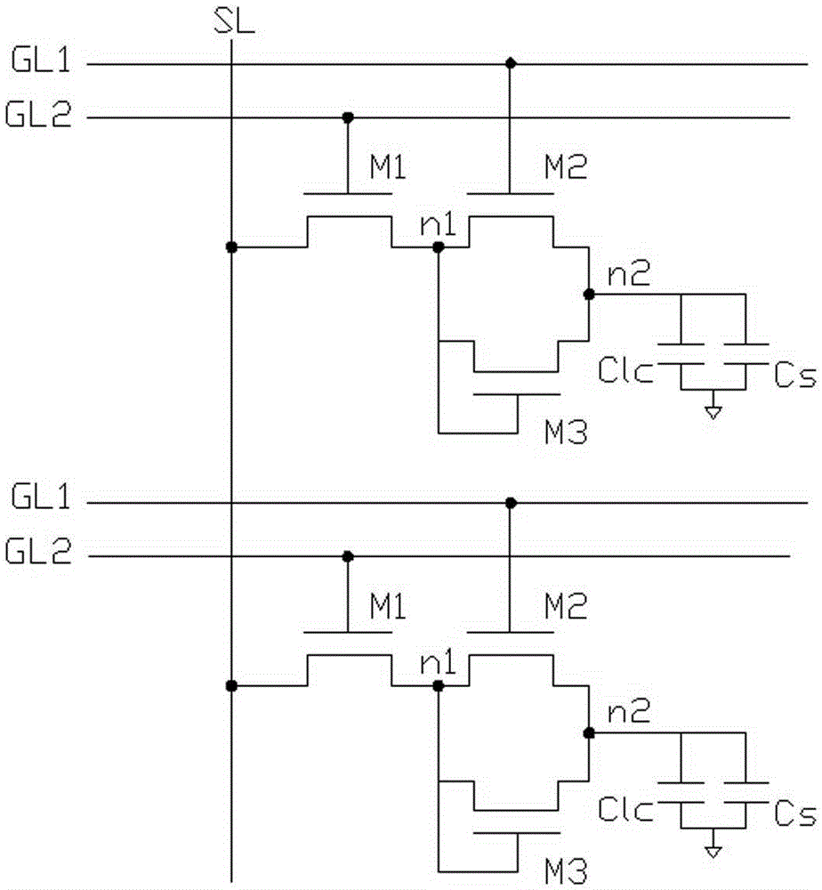
[0018] figure 1 It shows a pixel driving circuit of a preferred embodiment of the present invention, which is used in a liquid crystal display device, including a first gate line GateLine1 (GL1), a second gate line GateLine2 (GL2), a data line SourceLine (SL), a second gate line A transistor M1, a second transistor M2, a third transistor M3 and a pixel electrode.

[0019] The first transistor M1 is controlled in response to the second gate signal from the second gate line GateLine2 (GL2), and the first transistor M1 is connected between the data line SourceLine (SL) and the first node n1 , that is, the first transistor M1 is turned on or off according to the logic state of the second gate signal, and the data line SL and the first node n1 are electrically connected to each other when the first transistor M1 is turned on. The first transistor M1 has a gate terminal connected to the second gate line GL2, a source terminal connected to the data line SL, and a drain terminal conn...

Embodiment 2

[0028] An array substrate, which includes several pixel units distributed in a matrix, and also includes the pixel driving circuit as described in Embodiment 1.

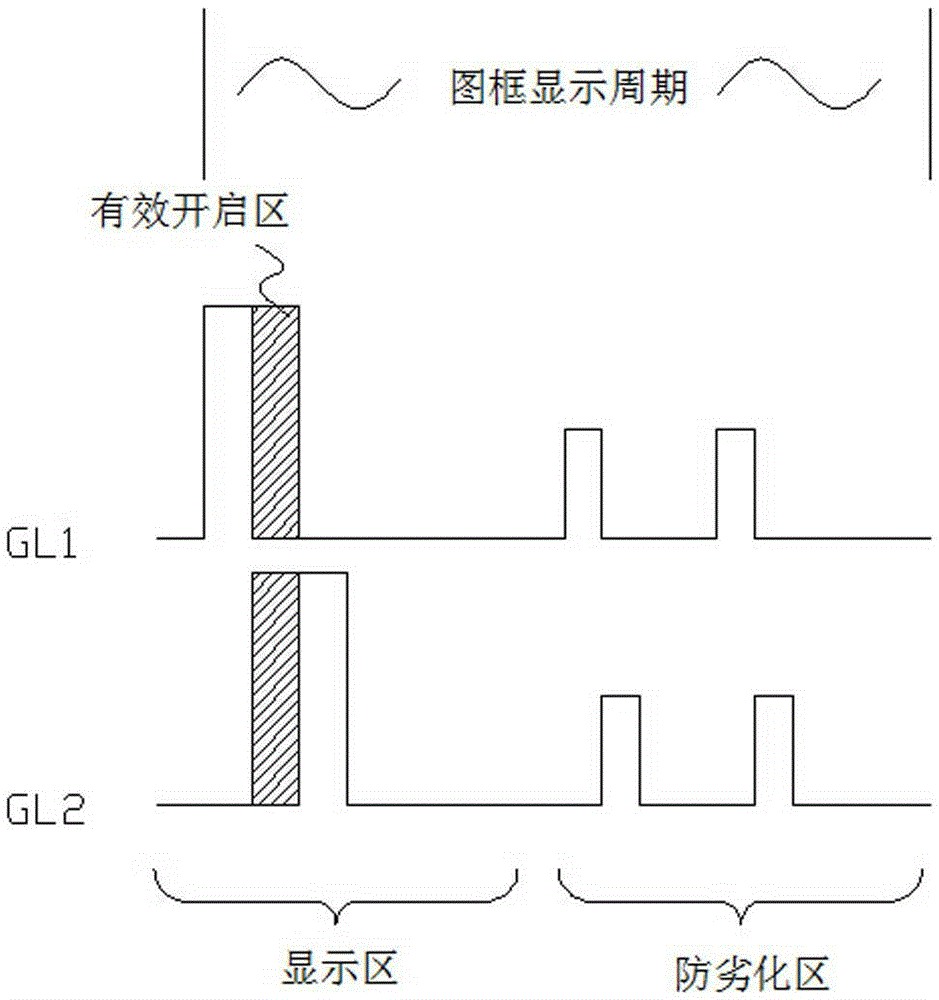
[0029] The array substrate of this embodiment, through the structure of three transistors, can increase the resistance of the switch circuit, reduce the leakage current, facilitate the maintenance of the display picture, and reduce the deterioration effect on the transistor under the low frequency driving signal. In the anti-deterioration area, use the normal driving frequency (such as 60Hz) to turn on one of the transistors independently, which can prevent the transistor from deteriorating, and at the same time, the transistor can also be turned off to prevent pixel leakage and will not affect the display quality.

Embodiment 3

[0031] A liquid crystal display device, comprising the array substrate as described in Embodiment 2. Specifically, the liquid crystal display device may be any product or component with a display function such as a liquid crystal panel, a mobile phone, a tablet computer, a television set, a display area, a notebook computer, a digital photo frame, and a navigator. The display mode of the liquid crystal display device is any one of a normally positive display mode, a normally black display mode, a transmissive mode, a transflective mode, and a full inversion mode.

[0032] The liquid crystal display device of this embodiment, through the structure of three transistors, can increase the resistance of the switch circuit, reduce the leakage current, facilitate the maintenance of the display screen, and reduce the deterioration effect on the transistor under the low frequency driving signal. In the anti-deterioration area, use the normal driving frequency (such as 60Hz) to turn on ...


PUM


Abstract

The invention discloses a pixel driving circuit which comprises a pixel driving circuit body, wherein the pixel driving circuit body comprises a first gating line, a second gating line, a data line, a first transistor, a second transistor, a third transistor and a pixel electrode. The invention further comprises an array substrate capable of displaying pixels by utilizing the pixel driving circuit and a liquid crystal display device. Through adoption of a structure comprising the three transistors, the switching circuit resistance can be increased, the leakage current is reduced, and keeping of a display image is facilitated; under a low-frequency driving signal, the deterioration effect on the transistors is reduced; the problems that the turn-off time of the transistors is prolonged when the frequency of a display module is reduced in the conventional display panel, and the transistors are deteriorated and the leakage current is increased after continuous powering-up can be solved.

Description

technical field [0001] The invention relates to the field of liquid crystal display, in particular to a pixel driving circuit, an array substrate and a liquid crystal display device. Background technique [0002] With the popularity of wearable products, users have higher and higher requirements for power consumption of products, among which the display module is a factor that affects power consumption. In the prior art, because the transistor is turned on or off for a long time, the transistor will deteriorate and affect the normal display of the display module. However, the lower the frequency of the driving signal is, the longer the operation time of the gate line is, and the transistor is turned on or off. The longer it takes, the transistor will deteriorate. Contents of the invention [0003] In order to solve the above-mentioned deficiencies in the prior art, the present invention provides a new type of pixel drive circuit, which can increase the resistance of the s...

Claims


Application Information

Patent Timeline
Patent Type & Authority Applications(China)
IPC IPC(8): G02F1/1362G02F1/1368
CPCG02F1/136227G02F1/136286G02F1/1368
Inventor 李林柳发霖何基强黄柏青
Owner TRULY SEMICON
Why Eureka
Try Eureka