Organic light emitting diode (OLED) display panel, manufacturing method of OLED display panel and display device

A display panel and cover plate technology, which is applied in semiconductor/solid-state device manufacturing, electrical components, diodes, etc., can solve problems such as difficult process, short circuit of wiring, and unguaranteed yield rate, so as to reduce shading rate and adhesion High, improve the effect of display efficiency

Active Publication Date: 2018-02-16
BOE TECH GRP CO LTD
View PDF2 Cites 14 Cited by
  • Summary
  • Abstract
  • Description
  • Claims
  • Application Information

AI Technical Summary

Problems solved by technology

Manufacturing the auxiliary electrodes on the backplane is not only difficult to realize in terms of technology, but also faces the risk of short circuit, and the yield rate cannot be guaranteed.

Method used


Image

  • Organic light emitting diode (OLED) display panel, manufacturing method of OLED display panel and display device
  • Organic light emitting diode (OLED) display panel, manufacturing method of OLED display panel and display device
  • Organic light emitting diode (OLED) display panel, manufacturing method of OLED display panel and display device

Examples


Embodiment Construction

[0044] The following will clearly and completely describe the technical solutions in the embodiments of the present invention with reference to the accompanying drawings in the embodiments of the present invention. Obviously, the described embodiments are only some, not all, embodiments of the present invention. Based on the embodiments of the present invention, all other embodiments obtained by persons of ordinary skill in the art without making creative efforts belong to the protection scope of the present invention.

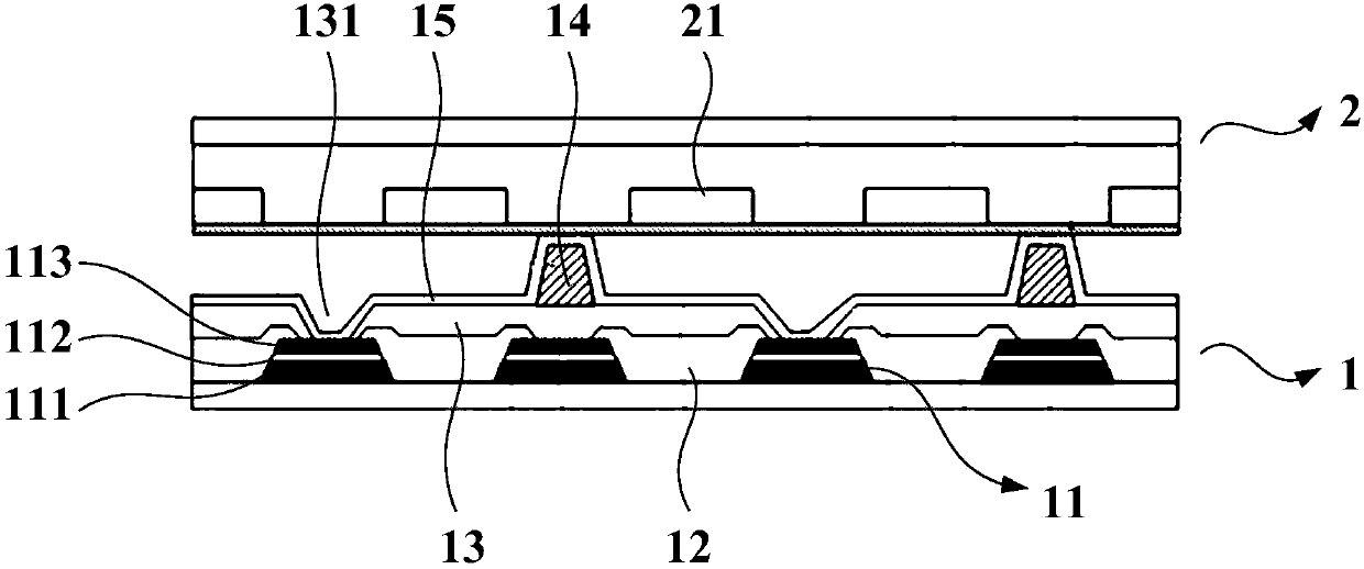
[0045] Please refer to figure 1 , the OLED display panel provided by the embodiment of the present invention includes a cover plate 1 and a back plate 2 arranged on the box, wherein:

[0046] A plurality of color filter units 12 are arranged in an array on the cover plate 1, and the gaps between each color filter unit 12 are filled with auxiliary cathodes 11, and the auxiliary cathodes 11 include a black matrix 111, a buffer layer 112 and metal layer 113;

...


PUM


Abstract

The invention discloses an organic light emitting diode (OLED) display panel, a manufacturing method of the OLED display panel and a display device. The process step is simplified, the yield is improved, and the display efficiency is improved. The OLED display panel comprises a cover plate, a back panel and a transparent electrode layer, wherein the cover plate and the back panel are buckled, a plurality of color film units are arranged on the cover plate in an array way, gaps among the color film units are filled with auxiliary negative electrodes, each auxiliary negative electrode comprisesa black matrix, a buffer layer and a metal layer which are sequentially formed on the cover plate, a flat layer is formed on the auxiliary negative electrodes and the color film units, a plurality ofholes are formed in positions, corresponding to the auxiliary negative electrodes, of the flat layer, a plurality of cushion pads are formed at positions, corresponding to the auxiliary negative electrodes, of the flat layer and are arranged between the cover plate and the back panel in a prop-against way, the transparent electrode layer is formed on the flat layer and the cushion pads, penetratethrough at least one part of holes and communicate with the auxiliary negative electrodes, and a color film layer of the cover and a pixel region of the back panel are arranged opposite to each other.

Description

technical field [0001] The present invention relates to the field of display technology, in particular to an organic light-emitting diode (Organic Light-Emitting Diode, OLED) display panel, a method for manufacturing the OLED display panel, and a display device. Background technique [0002] Due to its thinness, lightness, wide viewing angle, active luminescence, continuously adjustable luminous color, low cost, fast response, low energy consumption, low driving voltage, wide operating temperature range, simple production process, high luminous efficiency and Flexible display and other advantages have been listed as a promising next-generation display technology. [0003] In order to realize the manufacture of high-pixel display screens and obtain high-definition and high-fidelity display images, the industry has proposed a scheme of combining Oxide BP with printed OLEDs to achieve top emission. The inventors found that because the top emission needs to cooperate with the p...

Claims


Application Information

Patent Timeline
Patent Type & Authority Applications(China)
IPC IPC(8): H01L27/32H01L51/56H01L51/52
CPCH10K59/00H10K59/131H10K50/824H10K71/00H10K59/38H10K59/1275H10K59/1315H10K50/8428H10K50/865H10K50/828
Inventor 宋振王国英刘凤娟
Owner BOE TECH GRP CO LTD
Why Eureka
Try Eureka