Bendable display panel and manufacturing method thereof

A manufacturing method and display panel technology, applied to semiconductor devices, electrical components, circuits, etc., can solve the problems of display panel electrical signal loss, difficulty in climbing, and disconnection, so as to avoid loss of electrical signals, improve climbing ability, The effect of improving quality

Active Publication Date: 2020-09-04
WUHAN CHINA STAR OPTOELECTRONICS SEMICON DISPLAY TECH CO LTD
View PDF8 Cites 0 Cited by
  • Summary
  • Abstract
  • Description
  • Claims
  • Application Information

AI Technical Summary

Problems solved by technology

[0005] The main technical problem to be solved by this application is to provide a bendable display panel and its manufacturing method, so as to solve the difficulty in climbing the metal wiring at the DH step in the prior art, the poor coverage of the step, and the metal wiring at the step. The metal wiring in the area is much thinner, and it is prone to disconnection, resulting in an open circuit, which causes the technical problem of losing the electrical signal of the entire display panel

Method used


Image

  • Bendable display panel and manufacturing method thereof
  • Bendable display panel and manufacturing method thereof
  • Bendable display panel and manufacturing method thereof

Examples


Embodiment Construction

[0025] The technical solutions in the embodiments of the present application will be clearly and completely described below in conjunction with the drawings in the embodiments of the present application.

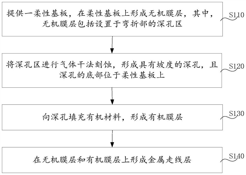
[0026] see image 3 , image 3 It is a schematic flowchart of the first embodiment of the manufacturing method of the bendable display panel of the present application. It should be noted that if there are substantially the same results, the method of the present application does not image 3 The flow sequence shown is limited. like image 3 As shown, the method includes the following steps:

[0027] Step S110: providing a flexible substrate, and forming an inorganic film layer on the flexible substrate, wherein the inorganic film layer includes a deep hole area disposed at the bending portion.

[0028] In this step, a bendable flexible substrate is provided first. Usually, the material of the flexible substrate adopts polymer materials such as polyimide plastic, polye...


PUM

PropertyMeasurementUnit
thicknessaaaaaaaaaa

Abstract

The present application discloses a bendable display panel and a manufacturing method thereof. The method includes: providing a flexible substrate, and forming an inorganic film layer on the flexible substrate, wherein the inorganic film layer includes a deep hole area arranged at the bending portion; The deep hole area is subjected to gas dry etching to form a deep hole with a slope, and the bottom of the deep hole is located on the flexible substrate; the deep hole is filled with organic materials to form an organic film layer; formed on the inorganic film layer and the organic film layer Metal trace layer. The method forms a deep hole with a slope by gas dry etching, and the etching method can control the slope of the deep hole, thereby improving the climbing ability of the metal wiring and reducing or avoiding the breakage of the display panel caused by the disconnection of the metal wiring. The phenomenon of electrical signal loss improves the quality of the display panel.

Description

technical field [0001] The present application relates to the field of display technology, in particular to a bendable display panel and a manufacturing method thereof. Background technique [0002] OLED (Organic Light-Emitting Diode, Organic Light-Emitting Diode) display has quickly occupied the high-end market of display panels due to its advantages of high contrast, wide color gamut, wide viewing angle, thinner and lighter, etc. With the continuous improvement of shortcomings, it is foreseeable that OLED displays will become the mainstream. Another advantage of the OLED display is that it can be bent, folded, and rolled, which makes it widely used in curved screens, foldable screens, or narrow-frame (borderless) screens. [0003] At present, many narrow-frame OLED mobile phone screens have appeared on the market, and their design concepts are similar, such as figure 1 or figure 2 In the two embodiments shown, the display screen adopts a flexible substrate of polymer m...

Claims


Application Information

Patent Timeline
Patent Type & Authority Patents(China)
IPC IPC(8): H01L27/32
CPCH10K59/131H10K59/1201
Inventor 卜呈浩
Owner WUHAN CHINA STAR OPTOELECTRONICS SEMICON DISPLAY TECH CO LTD
Why Eureka
Try Eureka