A tapered array broadband absorber and its preparation method

An absorber and cone technology, which is applied to the field of tapered array broadband absorbers and their preparation, can solve the problems of inability to prepare small-sized broadband absorbers in a large area, and achieve the effect of a simple preparation method.

Active Publication Date: 2020-09-29
SHENZHEN INLIGHT TECH CO LTD
View PDF7 Cites 0 Cited by
  • Summary
  • Abstract
  • Description
  • Claims
  • Application Information

AI Technical Summary

Problems solved by technology

[0006] In view of the above-mentioned deficiencies in the prior art, the object of the present invention is to provide a tapered array broadband absorber and its preparation method, aiming at solving the problem that the prior art cannot prepare a small-sized broadband absorber capable of absorbing visible light-infrared wavelength range in a large area. The problem

Method used


Image

  • A tapered array broadband absorber and its preparation method
  • A tapered array broadband absorber and its preparation method
  • A tapered array broadband absorber and its preparation method

Examples


preparation example Construction

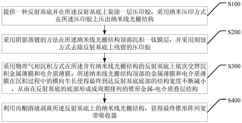
[0034] see figure 1 , figure 1 The flow chart of a preferred embodiment of the preparation method of a tapered array broadband absorber provided by the present invention, as shown in the figure, includes steps:

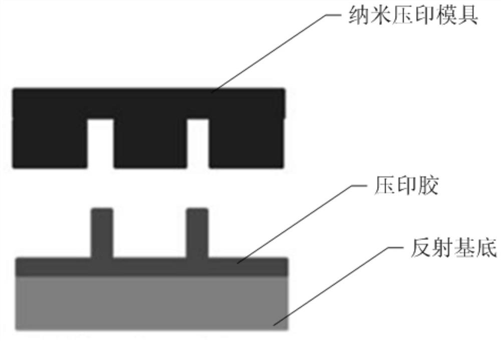
[0035] S100. Provide a reflective substrate and spin-coat a layer of embossing glue on the reflective substrate, and extrude a nanowire grating structure on the embossing glue by means of nanoimprinting;

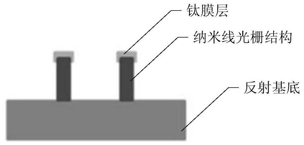
[0036] S200. Deposit a titanium film layer on the top of the nanowire grating structure by shadow evaporation, and remove the remaining embossing glue on the reflective substrate by etching;

[0037] S300. Alternately deposit a metal film and a dielectric film on the reflective substrate containing the nanowire grating structure by physical vapor deposition, and the lateral growth of the metal film and the dielectric film on the top of the nanowire grating structure during the deposition process makes the final The width of the structure reaching the bottom of the...


PUM

PropertyMeasurementUnit
widthaaaaaaaaaa
thicknessaaaaaaaaaa
widthaaaaaaaaaa

Abstract

The invention discloses a conical array broadband absorber and a preparation method therefor. The method comprises the steps of: extrudeing a nanowire grating structure on imprint adhesive on reflection substrate by adopting nanoimprint way; depositing a titanium film layer on top of the nanowire grating structure to remove the residual imprint adhesive on the reflection substrate; alternately depositing a metal thin film and a thin dielectric film on the reflection substrate in sequence, and using the phenomenon of natural lateral growth of the metal film and dielectric film during the deposition process, so that structure width eventually reaching the bottom of the reflective substrate continues to decrease, thus a periodically arranged conical metal-dielectric stack structure is formedat the bottom of the reflective substrate; and finally stripping the nanowire grating structure on the reflection substrate by using acetone solution to obtain the conical array broadband absorber. The preparation method provided by the invention is simple, rapid, and suitable for processing of large-area devices, and broadband absorption in visible light and infrared ranges is realized by the conical array broadband absorber.

Description

technical field [0001] The invention relates to the field of broadband absorbers, in particular to a tapered array broadband absorber and a preparation method thereof. Background technique [0002] In recent years, broadband absorbers have attracted widespread interest from researchers due to their important applications in infrared cloaking, light detection, heat detection, solar cells, broadband heat emitters, and reharvesting of exhaust heat in energy applications. . Some materials used in these applications (such as carbon nanotubes) can absorb light energy in a wide range of wavelengths, but the thickness of these structures is usually thick, on the order of microns, and the range of the absorbed spectrum cannot be effectively analyzed. Adjustment. [0003] In order to obtain a tunable broadband absorber, most researchers have proposed the concept of using a multi-resonant plasmonic structure, which can achieve the purpose of tuning the absorption wavelength by superi...

Claims


Application Information

Patent Timeline
Patent Type & Authority Patents(China)
IPC IPC(8): G02B5/00G02B1/00
CPCG02B1/002G02B5/003
Inventor 季陈纲
Owner SHENZHEN INLIGHT TECH CO LTD
Why Eureka
Try Eureka