Photoelectric detection substrate, preparation method thereof, and photoelectric detection device

A photoelectric detection and substrate technology, applied in the detection field, can solve the problems of high production cost and low yield rate.

Active Publication Date: 2018-12-25
BOE TECH GRP CO LTD
View PDF4 Cites 2 Cited by
  • Summary
  • Abstract
  • Description
  • Claims
  • Application Information

AI Technical Summary

Problems solved by technology

[0005] The technical problem to be solved by the embodiments of the present invention is to provide a photoelectric detection substrate and its pr

Method used


Image

  • Photoelectric detection substrate, preparation method thereof, and photoelectric detection device
  • Photoelectric detection substrate, preparation method thereof, and photoelectric detection device
  • Photoelectric detection substrate, preparation method thereof, and photoelectric detection device

Examples


Embodiment Construction

[0093] The specific implementation manners of the present invention will be further described in detail below in conjunction with the accompanying drawings and examples. The following examples are used to illustrate the present invention, but are not intended to limit the scope of the present invention. It should be noted that, in the case of no conflict, the embodiments in the present application and the features in the embodiments can be combined arbitrarily with each other.

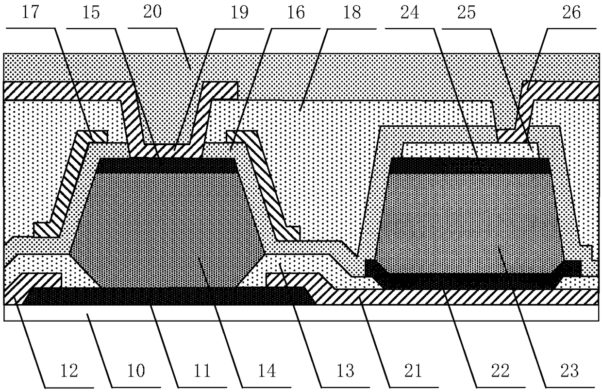
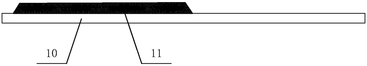
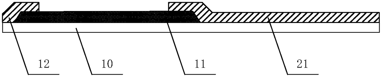
[0094] In order to overcome the defects of low yield rate and high production cost in the existing stacked structure of thin film transistors and photodiodes, an embodiment of the present invention provides a photodetection substrate. The main structure of the photodetection substrate includes a coplanar structure of thin film transistors and Photodiodes and thin film transistors are vertical channel structures. In the embodiment of the present invention, the coplanar structure of the thin film transi...


PUM


Abstract

The invention provides a photoelectric detection substrate, a preparation method thereof, and a photoelectric detection device. The photoelectric detection substrate comprises a thin film transistor and a photodiode having coplanar structure, and the thin film transistor is a vertical channel structure. By forming a coplanar structure of the thin film transistor with a vertical channel structure and the photodiode, the invention effectively reduces the overall thickness of the photoelectric detection substrate, reduces the deformation of the substrate caused by stress, avoids damage caused bythe deformation of the substrate, and improves the yield of the product. At the same time, because of the coplanar structure, the thin film transistor and the photodiode can be fabricated simultaneously, the number of times of the patterning process are reduced, the preparation process is simplified, and the production cost is reduced. As the occupied area of the vertical channel structure thin film transistor is small, the photodiode photosensitive area can be increased, so that the detection efficiency can be improve and the resolution of the product can be improved.

Description

technical field [0001] The invention relates to the technical field of detection, in particular to a photoelectric detection substrate, a preparation method thereof, and a photoelectric detection device. Background technique [0002] Photoelectric detection is widely used in medical, safety, non-destructive testing and other fields, and is increasingly playing an important role in the national economy and the people's livelihood. Detection, high-energy ion detection, environmental safety detection and other fields have been widely used. X-ray digital photography technology can be divided into direct conversion type (Direct DR) and indirect conversion type (Indirect DR). Because the indirect conversion type X-ray digital photography technology has the advantages of mature development, relatively low cost, and good device stability, it has been obtained extensive research. [0003] The main structure of the indirect conversion X-ray digital camera device includes a photodete...

Claims


Application Information

Patent Timeline
IPC IPC(8): H01L27/146
CPCH01L27/14616H01L27/14659H01L27/14689H01L27/14603H01L27/14663H01L27/14692
Inventor 黄睿杨昕周天民吴慧利
Owner BOE TECH GRP CO LTD
Why Eureka
Try Eureka