Flexible electronic device and manufacturing method thereof

A technology of flexible electronic devices and manufacturing methods, which is applied in the field of flexibility, and can solve the problems of poor energy absorption capacity, damage, and undeveloped wire stretching performance of flexible circuits, etc.

Active Publication Date: 2020-12-15
INST OF FLEXIBLE ELECTRONICS TECH OF THU ZHEJIANG +1
View PDF4 Cites 0 Cited by
  • Summary
  • Abstract
  • Description
  • Claims
  • Application Information

AI Technical Summary

Problems solved by technology

[0003] The characteristics of the current flexible substrate materials are stretchable, bendable, uniform force distribution and no directionality. This characteristic leads to the consistent force distribution of electronic devices and wires, which can straighten the flexible substrate and flexible wires. No fracture will occur under the condition of a large range of deformation, but the flexible circuit in the flexible electronic device will be damaged in a small range of deformation
This situation leads to the fact that under the action of external force, the flexible circuit is saturated and the stretching performance of the wire has not yet been exerted.
Secondly, under the impact of external force, the flexible circuit is thicker than the wire. First, it can withstand more impact force, but the relative energy absorption capacity of the flexible circuit is relatively poor, and it is easy to break and fail under the impact of external force.
In the prior art, in order to ensure that the flexible circuit is not damaged under impact, it is necessary to make a thicker flexible protective layer, which increases the thickness of the flexible electronic device on the one hand, and on the other hand affects the bending performance of the flexible electronic device. make an impact
Therefore, the property that flexible circuits are prone to breakage under impact has become a major factor limiting the development of flexible electronics.

Method used


Image

  • Flexible electronic device and manufacturing method thereof
  • Flexible electronic device and manufacturing method thereof
  • Flexible electronic device and manufacturing method thereof

Examples


Embodiment Construction

[0027] In order to further explain the technical means and functions adopted by the present invention to achieve the intended invention purpose, the detailed description is as follows in conjunction with the accompanying drawings and preferred embodiments.

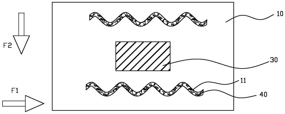
[0028] The invention provides a flexible electronic device, which can provide better shock resistance for circuits in the flexible electronic device while ensuring the bending performance.

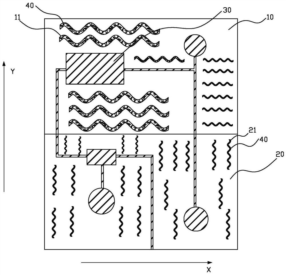
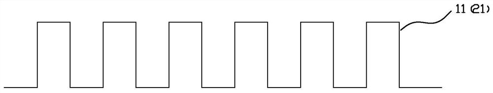
[0029] figure 1 Shown is a schematic diagram of the front structure of the flexible electronic device provided by the first embodiment of the present invention, such as figure 1 As shown, in the first embodiment of the present invention, the flexible electronic device includes a first flexible substrate 10, a circuit 30 and a first flow channel 11 are arranged on the first flexible substrate 10, and the first flow channel 11 extends in a meandering shape. The first flow channel 11 is filled with a non-Newtonian fluid 40 .

[0030] In...


PUM


Abstract

The invention provides a flexible electronic device and a fabrication method thereof. The flexible electronic device comprises a first flexible substrate, wherein a circuit and a first runner are arranged on the first flexible substrate, the first runner extends along a wriggling shape, and the first runner is filled with a non-Newtonian fluid. By the flexible electronic device, the bending performance is ensured, and relatively good impact-resistant capability can be provided for the circuit.

Description

technical field [0001] The invention relates to the field of flexible technology, in particular to a flexible electronic device and a method for manufacturing the flexible electronic device. Background technique [0002] As the core technology of future personalized wearable medical equipment, flexible electronics has received extensive attention and support from all sides. Flexible electronic devices (including circuits, sensors, electrodes, chips, etc.) have the advantages of good skin affinity, stretchability, and bendability as devices. At present, the demand for flexible electronic devices is not satisfied with functions such as bendable and stretchable. The research on flexible substrate materials is also an important part of the field of flexible electronics. [0003] The characteristics of the current flexible substrate materials are stretchable, bendable, uniform force distribution and no directionality. This characteristic leads to the consistent force distributio...

Claims


Application Information

Patent Timeline
Patent Type & Authority Patents(China)
IPC IPC(8): H01L23/02H05K5/06
CPCH01L23/02H05K5/067
Inventor 冯雪张柏诚唐瑞涛刘兰兰蒋晔
Owner INST OF FLEXIBLE ELECTRONICS TECH OF THU ZHEJIANG
Why Eureka
Try Eureka