Display substrate and manufacturing method thereof, display panel, display device

A technology of display substrate and substrate substrate, which is applied in static indicators, instruments, semiconductor devices, etc., can solve problems such as poor display effect and achieve good display effect.

Active Publication Date: 2022-02-11
BOE TECH GRP CO LTD
View PDF7 Cites 0 Cited by
  • Summary
  • Abstract
  • Description
  • Claims
  • Application Information

AI Technical Summary

Problems solved by technology

[0006] The object of the present invention is to overcome the disadvantages of the poor display effect of the above-mentioned prior art, and provide a display substrate with a better display effect, a method for preparing the display substrate, a display panel with the display substrate installed, and a display panel with the display panel installed. display device

Method used


Image

  • Display substrate and manufacturing method thereof, display panel, display device
  • Display substrate and manufacturing method thereof, display panel, display device
  • Display substrate and manufacturing method thereof, display panel, display device

Examples


Embodiment Construction

[0075] Example embodiments will now be described more fully with reference to the accompanying drawings. Example embodiments, however, can be embodied in various forms and should not be construed as limited to the embodiments set forth herein; rather, these embodiments are provided so that this disclosure will be thorough and complete, and will fully convey the concept of example embodiments to those skilled in the art. The same reference numerals in the drawings denote the same or similar structures, and thus their detailed descriptions will be omitted.

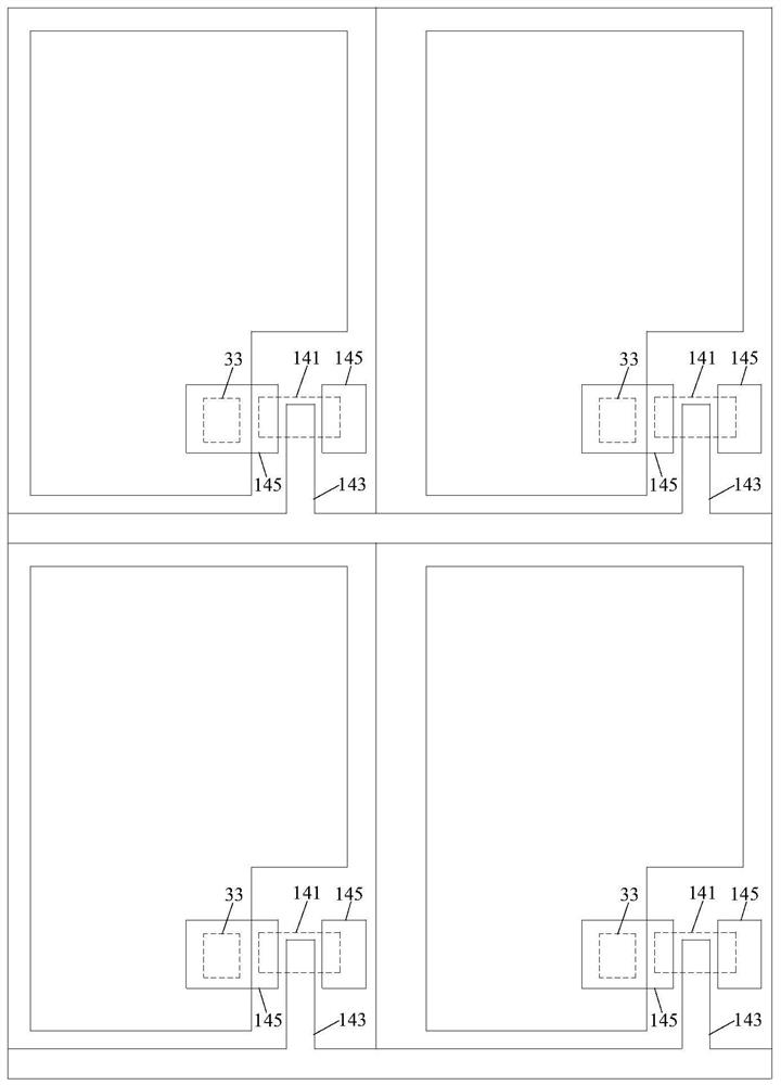
[0076] The OLED display panel may include: a cover plate and a back plate. refer to figure 1 The schematic diagram of the arrangement structure of the optical detection device and the optical compensation control TFT in the related art shown; in each sub-pixel region in the cover plate, an optical compensation control TFT (English: Thin Film Transistor, abbreviation: TFT, Chinese abbreviation can be provided) : thin film ...


PUM


Abstract

The invention relates to the field of display technology, and provides a display substrate and a preparation method thereof, a display panel, and a display device. The preparation method of the display substrate includes: forming an optical compensation control thin film transistor on one side of the base substrate; forming a conductor protection layer on the side of the optical compensation control thin film transistor away from the base substrate; Form an optical detection device material layer on one side; pattern the optical detection device material layer to form an optical detection device, and pattern the conductor protection layer to form a conductor pattern; wherein, the optical detection device controls the source of the thin film transistor through the conductor pattern and optical compensation pole or drain electrical connection. After using this method, the display effect of the display panel is better.

Description

technical field [0001] The present invention relates to the field of display technology, and in particular, to a display substrate and a method for preparing the display substrate, a display panel mounted with the display substrate, and a display device mounted with the display panel. Background technique [0002] An organic light emitting diode (English: Organic light emitting diode; OLED for short) display panel is a new type of display panel on the market. Compared with liquid crystal display panels, OLED display panels have many advantages such as wide color gamut, high contrast ratio, and ultra-thinness due to the self-luminous properties of OLED display panels. [0003] Since the OLED display panel works in a state of high contrast and high brightness for a long time, the luminous brightness of the organic light-emitting layers in each sub-pixel in the OLED display panel is inconsistent, which will cause the OLED display panel to emit unevenly. The sub-pixels in the d...

Claims


Application Information

Patent Timeline
Patent Type & AuthorityPatents(China)
IPC IPC(8): H01L27/32
CPCH10K59/60H10K59/126H10K71/00H10K71/20G09G3/3225H10K59/131
Inventor王国英宋振
OwnerBOE TECH GRP CO LTD