Thin film transistor, preparation method thereof, array substrate, display panel and device

A technology of thin film transistors and display devices, applied in the direction of transistors, semiconductor/solid-state device manufacturing, semiconductor devices, etc., can solve the problems of increasing TFT hole capture probability, device threshold voltage drop, leakage current increase, etc., to reduce hole The effect of producing, reducing concentration and improving performance

Pending Publication Date: 2019-12-27
HEFEI XINSHENG OPTOELECTRONICS TECH CO LTD +1
View PDF4 Cites 0 Cited by
  • Summary
  • Abstract
  • Description
  • Claims
  • Application Information

AI Technical Summary

Problems solved by technology

[0003] Considering the working environment, the on-board display must be able to withstand the high and low temperature difference between -30°C and +85°C; and working in a high-temperature environment for a long time will incr...

Method used


Image

  • Thin film transistor, preparation method thereof, array substrate, display panel and device
  • Thin film transistor, preparation method thereof, array substrate, display panel and device
  • Thin film transistor, preparation method thereof, array substrate, display panel and device

Examples


Embodiment Construction

[0032] The following will clearly and completely describe the technical solutions in the embodiments of the present invention with reference to the accompanying drawings in the embodiments of the present invention. Obviously, the described embodiments are only some, not all, embodiments of the present invention. Based on the embodiments of the present invention, all other embodiments obtained by persons of ordinary skill in the art without making creative efforts belong to the protection scope of the present invention.

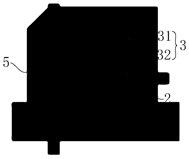
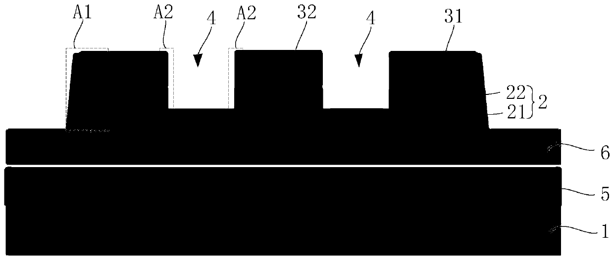
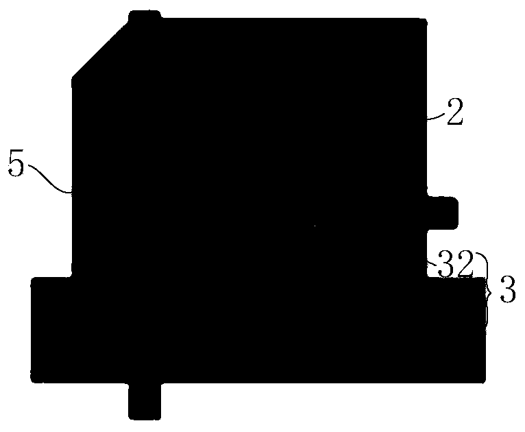
[0033] Such as Figure 1 to Figure 3 As shown, the embodiment of the present invention provides a thin film transistor, including a base substrate 1, an active layer 2 and a source-drain electrode 3 sequentially stacked on the base substrate 1; the source in the source-drain electrode 3 The projection of the electrode 31 on the base substrate 1 overlaps with the projection of part of the edge of the active layer 2 on the base substrate 1, as figure 2 Shown i...


PUM


Abstract

The invention belongs to the technical field of display and discloses a thin film transistor, a preparation method thereof, an array substrate, a display panel and a display device. The thin film transistor comprises a substrate, as well as an active layer and a source-drain electrode which are sequentially stacked on the substrate; and the projection of a source electrode in the source-drain electrode on the substrate is overlapped with the projection of part of the edge of the active layer on the substrate. According to the thin film transistor, the illumination-receiving area of the activelayer is small, so that the generation of holes can be effectively reduced, the concentration of photon-generated carriers under an illumination condition is reduced, and therefore, the defect statessuch as hole capture probability increase and threshold voltage reduction, of the TFT working in a high-temperature illumination environment are avoided, and the performance of the TFT device in the high-temperature illumination environment is improved. When the thin film transistor is applied to the display panel, the working performance of the display product in a high-temperature environment can be improved, and the reliability of the display product is enhanced.

Description

technical field [0001] The invention relates to the field of display technology, in particular to a thin film transistor and a preparation method thereof, an array substrate, a display panel and a device. Background technique [0002] In recent years, with the expansion of display panel production capacity, the consumer market has grown slowly. Therefore, finding new fast-growing application fields has become an urgent need for major manufacturers. With the rapid development of the automobile market and the advent of the Internet of Vehicles era, the field of vehicle display has obviously become the third largest application market for small and medium-sized panels after the mobile phone and tablet market. [0003] Considering the working environment, the on-board display must be able to withstand the high and low temperature difference between -30°C and +85°C; and working in a high-temperature environment for a long time will increase the hole capture probability of the TFT...

Claims


Application Information

Patent Timeline
IPC IPC(8): H01L29/786H01L21/336
CPCH01L29/78633H01L29/66742H01L29/41733H01L27/1214H01L29/41783H01L29/66765H01L29/78618
Inventor 陈川陈鹏宇马涛杨成绍
Owner HEFEI XINSHENG OPTOELECTRONICS TECH CO LTD
Why Eureka
Try Eureka