
Plane display with touching function and its forming method
A flat-panel display and display element technology, applied in static indicators, instruments, electrical components, etc., can solve problems such as affecting the life and quality of display panels, difficult to balance display quality and touch performance, and lowering
- Summary
- Abstract
- Description
- Claims
- Application Information
AI Technical Summary
Problems solved by technology
Method used
Image

Examples
Embodiment Construction
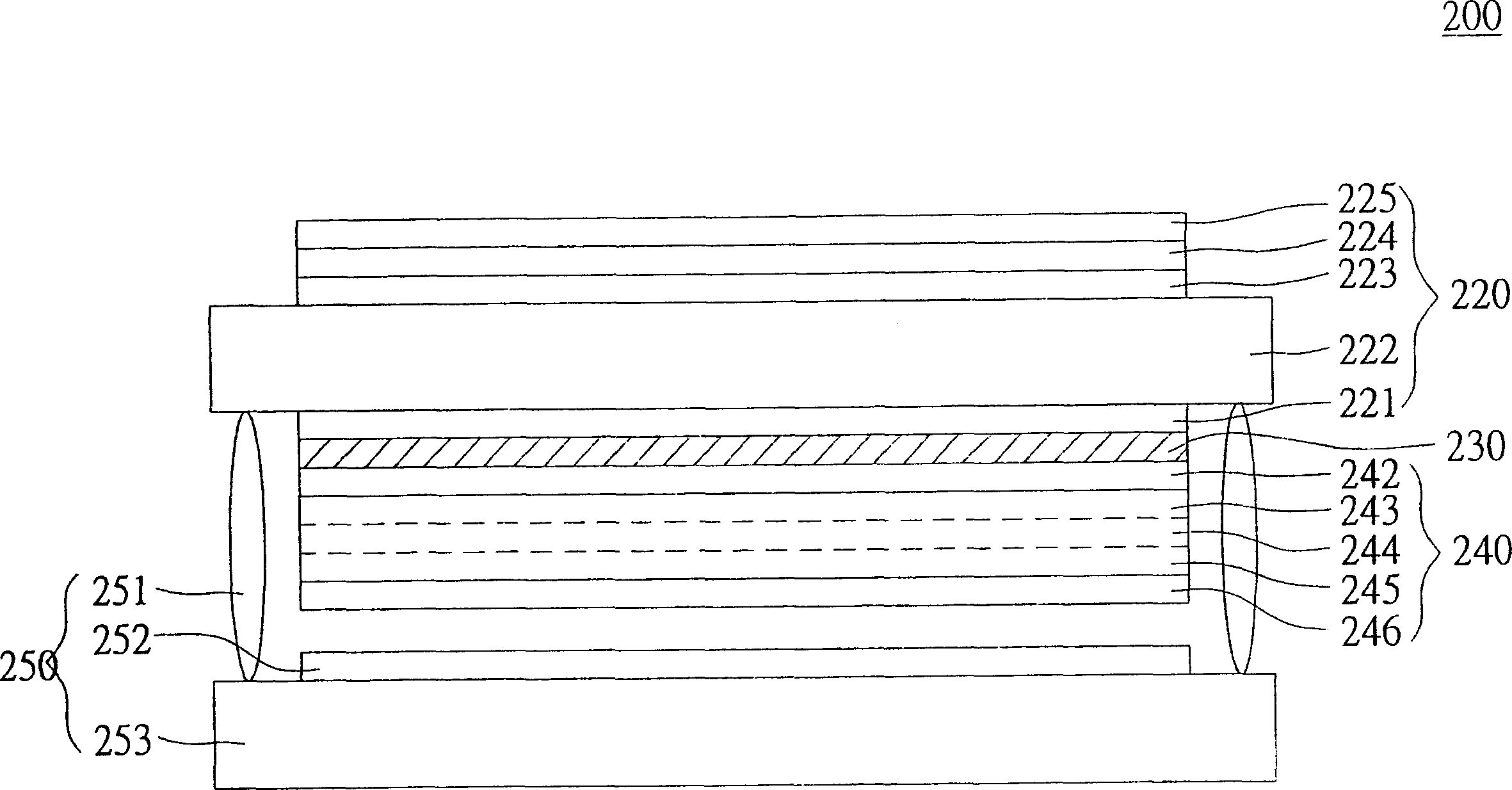
[0029] The main idea of the present invention is to directly form organic electroluminescent display elements on the surface of the capacitive touch panel, and the two are only separated by an insulating layer. The thickness and weight of the flat-panel display can be reduced, and the display quality of the display and the touch performance of the touch panel can be taken into consideration.
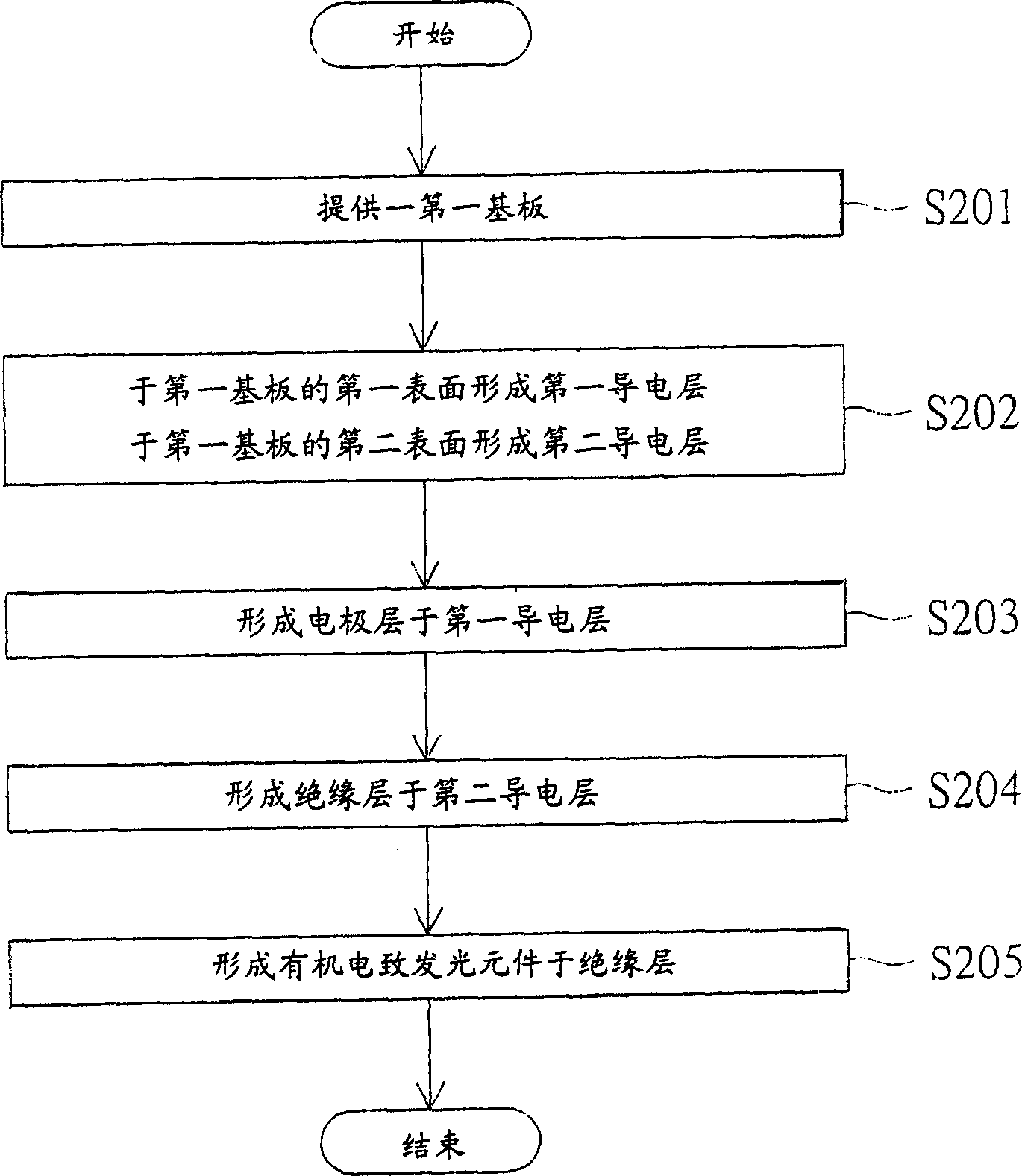
[0030] The plane display of the present invention includes a first substrate, a first conductive layer, a second conductive layer, an electrode layer, an insulating layer and an organic electroluminescence display element. The first conductive layer is formed on the first surface of the first substrate, and the electrode layer is formed on the first conductive layer. The second conductive layer is formed on the second surface of the first substrate, the insulating layer is formed on the surface of the second conductive layer, and the organic electroluminescence display element is forme...
PUM
 Abstract
Description
Claims
Application Information