Array substrate and manufacturing method thereof

An array substrate and manufacturing method technology, applied in the field of touch screens, can solve the problems of high manufacturing cost, complex process flow, and restrictions on extensive development, and achieve the effects of improving the yield rate, simplifying the manufacturing process, and reducing costs

Active Publication Date: 2017-10-20
NANJING CEC PANDA FPD TECH CO LTD
View PDF5 Cites 5 Cited by
  • Summary
  • Abstract
  • Description
  • Claims
  • Application Information

AI Technical Summary

Problems solved by technology

[0004] However, for the design of the existing embedded touch screen array substrate, the structure of each film layer and the process flow are relatively complicated, and the number of masks is large, which leads to high preparation costs and limits its extensive development.

Method used


Image

  • Array substrate and manufacturing method thereof
  • Array substrate and manufacturing method thereof
  • Array substrate and manufacturing method thereof

Examples


Embodiment

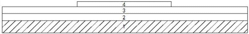
[0029] Embodiment: an array substrate, the specific manufacturing process is as follows:

[0030] Step 1: As shown in Figure 1(a), on the substrate Glass 1, the gate line Gate 2 metal layer is formed on the substrate Glass 1 by means of film formation, exposure, development, and etching, and is connected to the gate line Gate 2 The grid, the first metal wire is a single-layer film of aluminum, molybdenum, copper, titanium, chromium, neodymium or a composite film of any combination thereof.

[0031] Step 2: As shown in FIG. 1(b), form a thin film of the gate insulating layer GI 3 on the metal layer of the gate line Gate 2. The material can be a single body of silicon oxide or silicon nitride, or a combination of both, Approx. The pattern of oxide semiconductor OS 4 is formed on the gate insulating layer GI3 by means of film formation, exposure, development, and etching. The semiconductor is not limited to InGaZnO, but can also be completed by other oxide semiconductor materia...


PUM


Abstract

The invention provides an array substrate and manufacturing method thereof. The array substrate includes a gate line and a data line which are crisscrossed, a touch control wire, a plurality of pixel regions defined by intersection of the gate line and the data line, a TFT switch at the intersection of the gate line and the data line, a gate insulation layer located on the gate line, an oxide semiconductor located on the gate insulation layer, a first insulation layer that covers the oxide semiconductor and the data line, a third insulation layer that covers the first insulation layer, pixel electrodes located on the third insulation layer and located in the pixel regions, a pad layer located under the touch control wire, a second insulation layer that covers the touch control wire and pixel electrodes, and a plurality of common electrodes located on the second insulation layer. The array substrate uses a gray scale mask plate, through a reduced number of mask processes, the array substrate having a touch control function is prepared, and compared with a conventional design, the array substrate preparation process is obviously simplified, the yield of array substrates is improved, and the cost is reduced.

Description

technical field [0001] The invention relates to a touch screen, in particular to an array substrate and a manufacturing method thereof. Background technique [0002] Since the iPhone 4 adopts a capacitive touch screen, the public's requirements for the touch screen experience have also increased, and the touch screen has become the mainstream in the display field. [0003] Currently, the most widely used touch panels are Add on Touch Panels that are mounted outside the display screen and In cell Touch Panels that are embedded in the display screen. The built-in touch screen integrates the touch function inside the LCD, which greatly meets the needs of consumers for thinner displays, and is also synonymous with high-end products. [0004] However, for the design of the existing embedded touch screen array substrate, the structure of each film layer and the process flow are relatively complicated, and the number of masks is large, which leads to high preparation costs and lim...

Claims


Application Information

Patent Timeline
Patent Type & Authority Applications(China)
IPC IPC(8): H01L27/12H01L21/77
CPCH01L27/124H01L27/1288
Inventor 张甜舒强
Owner NANJING CEC PANDA FPD TECH CO LTD
Why Eureka
Try Eureka