
Semi-insulating silicon carbide without vanadium domination
a silicon carbide and silicon carbide technology, applied in the microwave field, can solve the problems of reducing yield, negatively affecting the crystalline quality of the resulting material, and generally too conductive silicon carbide grown by most techniques, and achieve the effect of high frequency operation
- Summary
- Abstract
- Description
- Claims
- Application Information
AI Technical Summary
Benefits of technology
Problems solved by technology
Method used
Image

Examples
Embodiment Construction
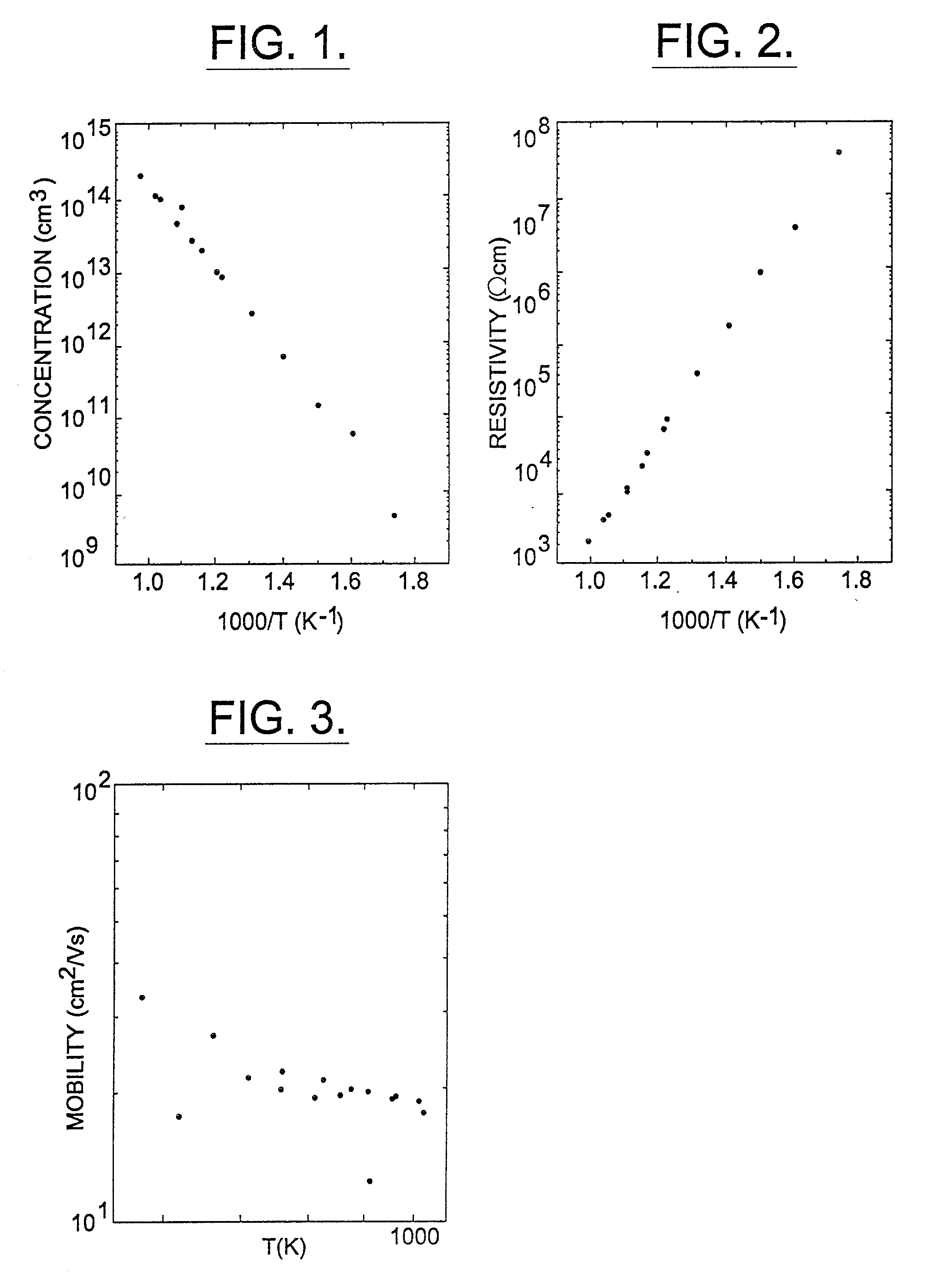
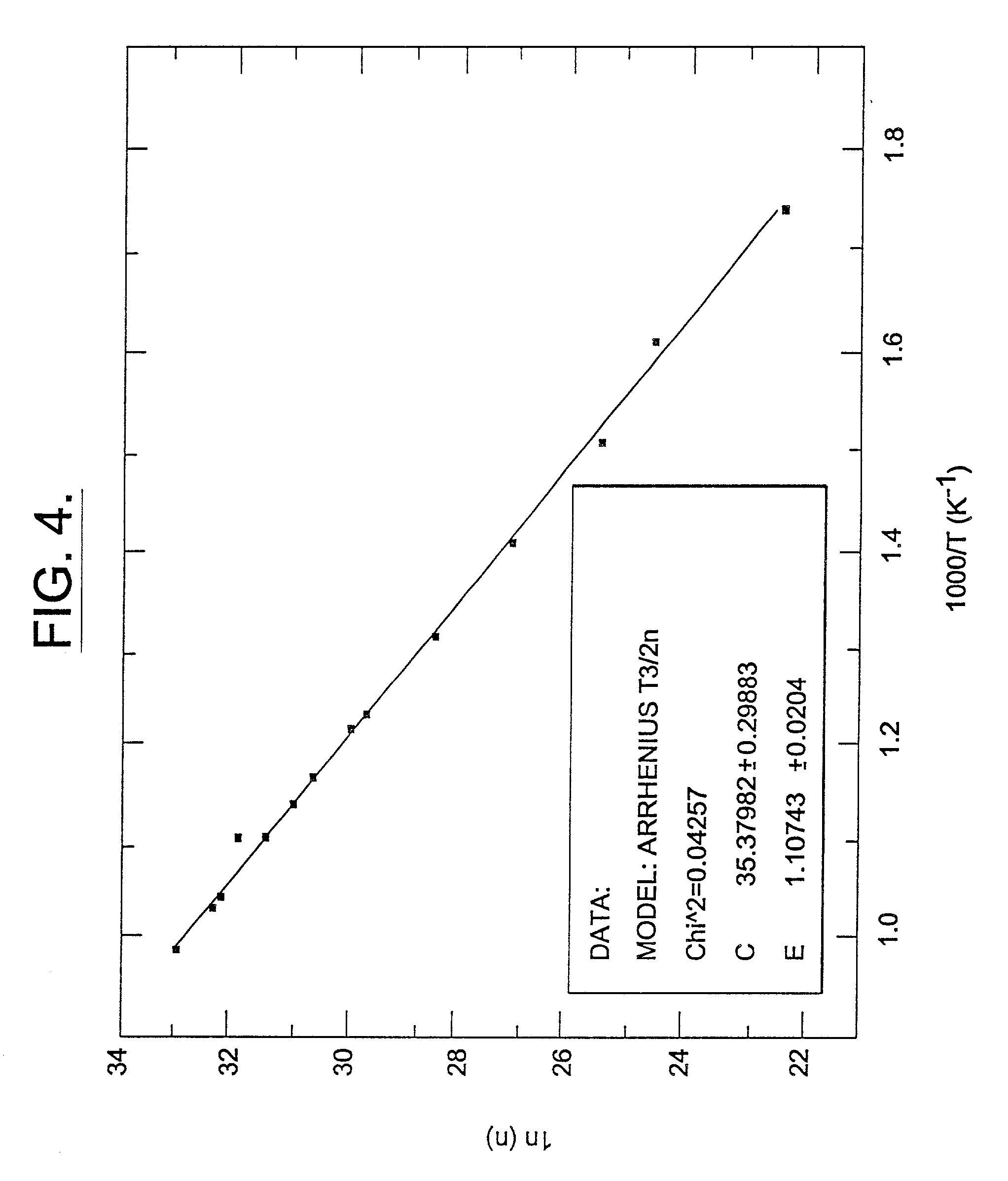
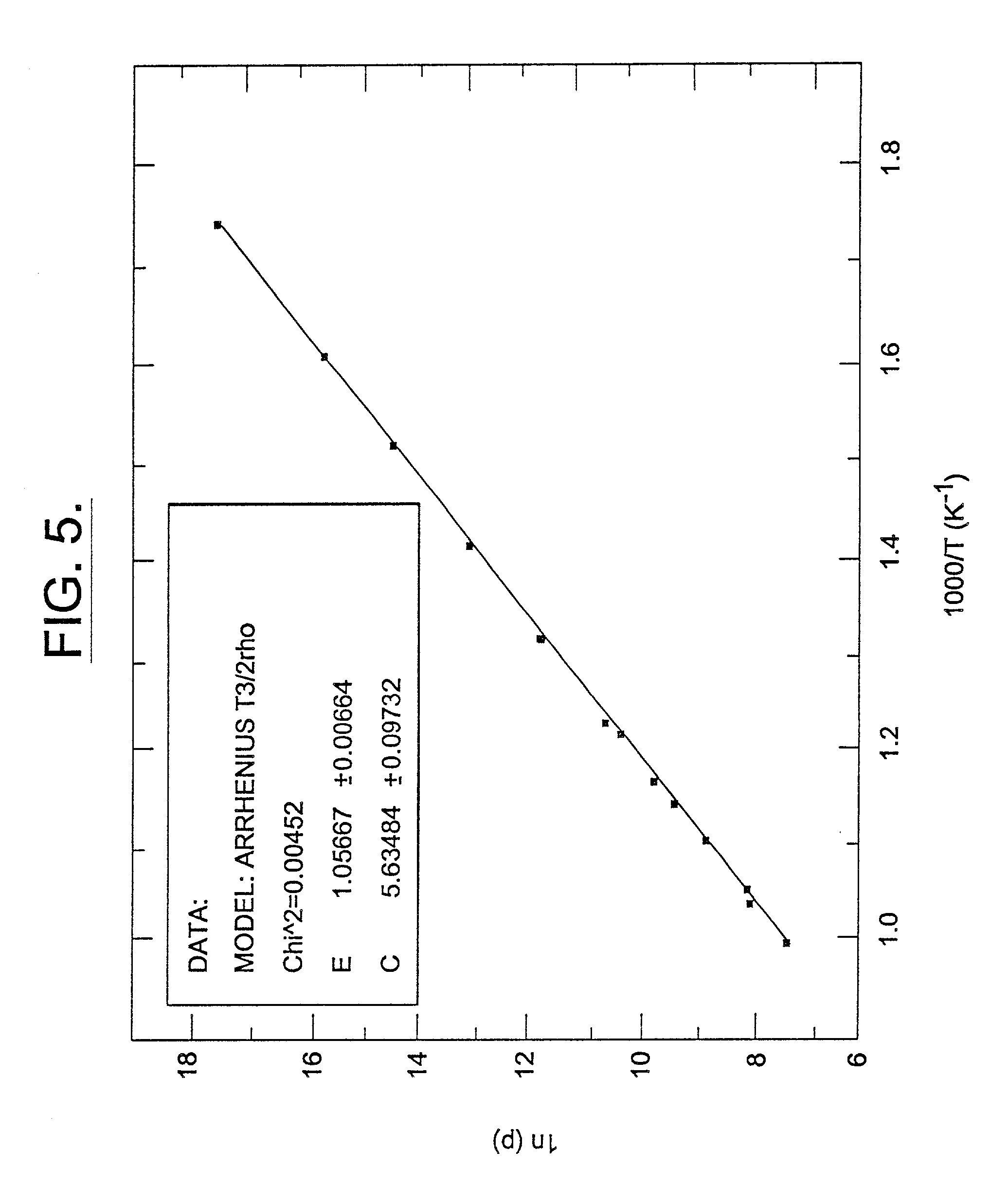
[0071] Two wafers of semi-insulating SiC were examined at the Air Force Research Laboratory at Dayton, Ohio (Wright-Patterson Air Force Base), with high temperature Hall effect and SIMS. No understandable results were available from one of the wafers (possibly because of unsatisfactory ohmic contacts), but two Hall samples from the second wafer both gave the same results, giving a reasonable confidence level in those results.
[0072] Both wafers were insulating at room temperature. The measurable wafer was thermally activated at elevated temperatures and the carrier concentration was measurable, which is not always possible in semi-insulating material because of the low mobilities due to the high temperatures involved. The carrier concentration was around 10.sup.15 cm.sup.-3 at 1000K where the resistivity was about 103 .OMEGA.-cm. Such carrier concentration is about one to two orders of magnitude lower than that seen in conventional semi-insulating material or vanadium doped material ...
PUM
| Property | Measurement | Unit |
|---|---|---|
| wavelengths | aaaaa | aaaaa |
| frequencies | aaaaa | aaaaa |
| temperature | aaaaa | aaaaa |
Abstract
Description
Claims
Application Information