Display unit and drive system thereof and an information display unit

a technology of information display unit and drive system, which is applied in the direction of static indicating device, cathode-ray tube indicator, instruments, etc., can solve the problems of increasing the cost of combining a common driver and a segment driver as one semiconductor chip, generating flickers, and difficult to combine a common driver and a segment driver as one chip. , to achieve the effect of effective suppression of flicker occurrence, good display and high contras

Active Publication Date: 2004-04-08
JAPAN DISPLAY CENT INC
View PDF6 Cites 370 Cited by
  • Summary
  • Abstract
  • Description
  • Claims
  • Application Information

AI Technical Summary

Benefits of technology

0011] According to another aspect of the present invention, regarding gradation data subject to a frame rate control (FRC), the first gradation data may be comprised of common divisors of 12 and the second gradation data may be comprised of common divisors of 8. By performing a gradation display with the gradation data, the flicker occurrence can be effectively suppressed. Also, a good display with a high contrast can be compatibly achieved both in display of a moving picture and a still picture.
0012] A gradation selection circuit may be provided on each segment (or source) signal line for selecting gradation data corresponding to image data based on the image data and output data of a gradation data shift circuit. Regarding gradation registers of the gradation data shift circuit, there is omitted a gradation register which can be formed by mirror reversion of the data, and the data of the omitted gradation register is restored by reversing the data of the gradation data shift circuit in the gradation selection circuit. By this arrangement, the circuit scale can be reduced to half and an IC chip size can be also reduced to thereby realize a reduction in cost.
0013] In specific, in a simple matrix type LCD panel, an amplitude of a selection signal for a common driver IC is much larger than an amplitude of a data signal for a segment driver IC. According to the present invention, a dummy pulse is superimposed on the data signal to thereby comparatively reduce the amplitude of the selection signal.
0014] Moreover, by carrying out a multi line selection (MLS) drive to be described later, the amplitude of the selection signal can be further reduced. By this arrangement, the amplitude difference between the selection s

Problems solved by technology

However, in a display panel using a liquid crystal layer as a light modulation layer, there arises a problem that flickers are generated when a frame rate (i.e., frames number to be rewritten on a display screen per a second) is lowered.
On the other hand, when a frame rate is made higher to suppress the occurrence of flickers, the circuit scale of the display unit is increased to be a problem.
Accordingly, a high tolerance voltage processing is required as an I

Method used


Image

  • Display unit and drive system thereof and an information display unit
  • Display unit and drive system thereof and an information display unit
  • Display unit and drive system thereof and an information display unit

Examples


embodiment 1

[0358] From FIG. 34, when the dummy pulse is set, the necessary tolerance voltage on both the signal and scanning sides decreases and the longer pulse width is made, the further it decreases. In particular, when the dummy pulse width is set at 0.075, the tolerance voltage on the signal side drops below 5V making 5V process applications such as the 0.35 .mu.m process possible. Furthermore, in embodiment 1, the ON / OFF ratio was 1.052, but in this embodiment it was found to have improved to 1.058.

embodiment 3

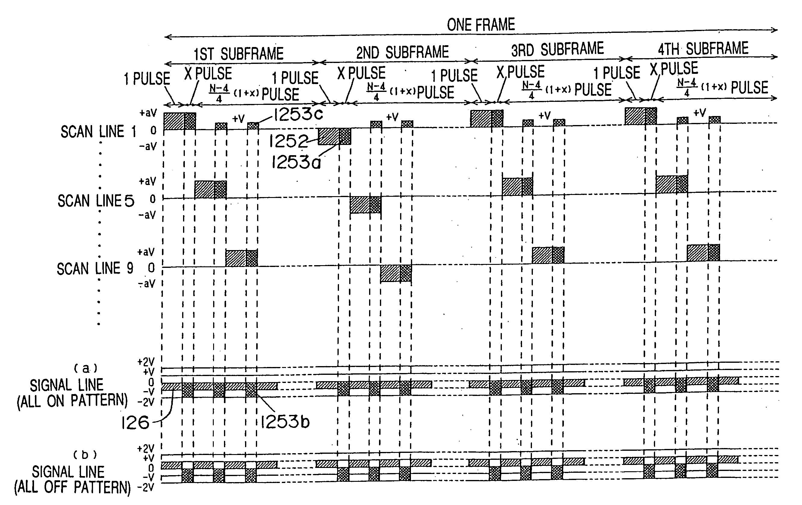
[0359] Using FIG. 35, the following explanation covers the state of embodiment 3 of the present invention. In this drawing, 1252 represents the spanning lines selected signal, 1261, the signal line drive waveform, 1253d, the scanning line dummy pulse and 1253e, the signal line dummy pulse.

[0360] In embodiment 3 of the present invention, as is shown in FIG. 35, the dummy pulse 1253d impressed onto the, scanning line, is characterized by the fact that the straight polarity (+aV) selected signals are applied at a certain pulse width to all scanning lines at once each time all of the scanning lines have been scanned (sub-frame).

[0361] The dummy pulse 1253e on the signal line of the present invention is impressed at the exact same pulse width and timing as the scanning line dummy pulse. Additionally, the voltage value of the dummy pulse impressed onto the signal line uses a reference voltage of (L / 2) V which is derived from a polarity with multiple selected signals of scanning electrodes...

embodiment 2

[0365] From FIG. 38, when the dummy pulse is set, the necessary tolerance voltage on both the signal and scanning sides decreases and the longer pulse width is made, the further it decreases. In particular, when the dummy pulse width is set at 0.4, the tolerance voltage on the signal side drops below 5V making 5V process applications such as the 0.35 .mu.m process possible. Furthermore, the ON / OFF ratio, which was 1.058 in embodiment 2, was found to have improved in this embodiment to 1.061.

[0366] As shown above, according to the drive method of the simple matrix-type display panel through the multiline select drive (MSL) which is the present invention's dummy pulse impressed onto the scanning and signal electrodes, it is possible to reduce the tolerance voltage required by the scanning and signal drive circuits. As a result, IC design by a conventional low tolerance voltage process becomes possible. In turn, this makes the realization of low power consumption and cost reduction pos...


PUM


Abstract

In a display panel, a dummy pulse of a predetermined voltage signal is superimposed on a data signal and the dummy pulse has an amplitude much larger than the amplitude of the data signal, and thus a signal waveform applied to a light modulation layer such as LC layer is changed to a high frequency wave. The applying position of the dummy pulse is varied according to each color of R, G and B, or varied according to frame or field. By performing a MLS drive with the dummy pulse superimposed on the data signal, the amplitude difference between the selection signal and the data signal can be reduced. Thus, a common driver IC and a segment driver IC can be formed as one semiconductor chip to be placed on one side, constructing a three side free type.

Description

[0001] The present invention relates to a display unit using a liquid crystal display (LCD) panel and the like that can achieve a high light-utilization efficiency in both a transparent mode and a reflective mode, and to a driving system therefor, and further relates to a portable information terminal device such as a viewfinder, video camera, and a mobile or portable telephone.[0002] Since LCD panels have the advantages of being slim and low power consumption, they are commonly used in many portable appliances such as word processors, personal computers and televisions, as well as the viewfinders and monitors of video cameras. In recent years, there has been adopted a reflective-type LCD panel using external light as a light source in place of backlight.[0003] However, in a display panel using a liquid crystal layer as a light modulation layer, there arises a problem that flickers are generated when a frame rate (i.e., frames number to be rewritten on a display screen per a second)...

Claims


Application Information

Patent Timeline
IPC IPC(8): G06F3/14G09G3/20G09G3/32G09G3/36G09G5/39
CPCG06F3/14G09G2360/18G09G3/2018G09G3/2051G09G3/32G09G3/3611G09G3/3625G09G3/3696G09G5/39G09G2310/0275G09G2310/06G09G2320/0209G09G2320/0247G09G2320/0276G09G2320/041G09G2320/0606G09G2320/0626G09G2320/0673G09G2330/021G09G3/20
Inventor YAMANO, ATSUHIROTAKAHARA, HIROSHITSUGE, HITOSHI
Owner JAPAN DISPLAY CENT INC
Why Eureka
Try Eureka