

Polishing method
a technology of polishing method and polishing plate, which is applied in the direction of lapping machines, manufacturing tools, semiconductor devices, etc., can solve the problems of short circuit, large step height on the surface of the semiconductor device, and complicated structure of the semiconductor element, so as to prevent the effect of being dropped off and damaged
- Summary
- Abstract
- Description
- Claims
- Application Information
AI Technical Summary
Benefits of technology
Problems solved by technology
Method used
Image

Examples
Embodiment Construction
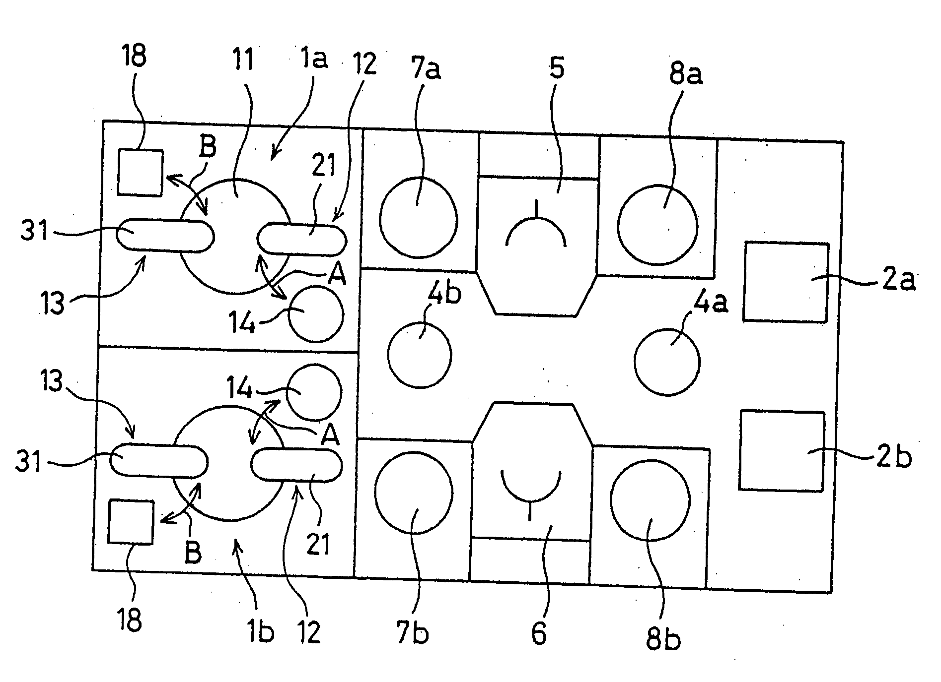
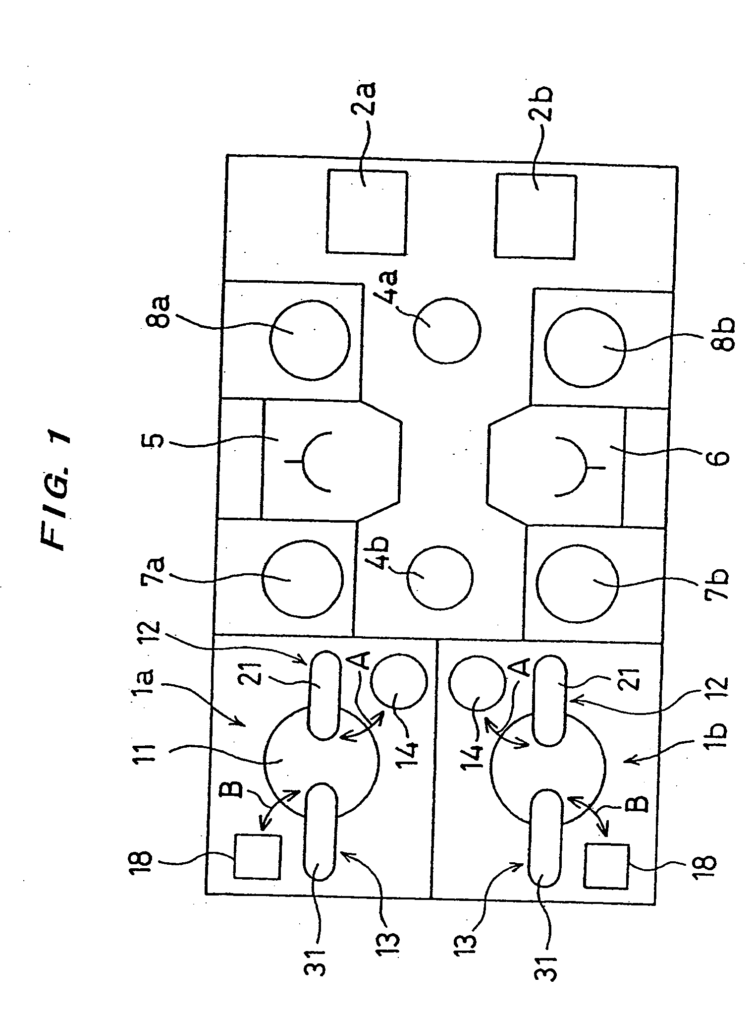
[0043] A polishing method according to a first embodiment of the present invention will be described below in detail with reference to FIGS. 1 through 12. FIG. 1 is a schematic plan view showing a polishing apparatus according to the first embodiment of the present invention. As shown in FIG. 1, in the polishing apparatus, a pair of polishing sections 1a, 1b are disposed at one side of a space on a floor having a rectangular shape so as to face each other. A pair of load / unload units for placing cassettes 2a, 2b thereon which accommodate semiconductor wafers are disposed at the other side. Two transfer robots 4a, 4b for transferring the semiconductor wafer are disposed on a line connecting the polishing sections 1a, 1b to the load / unload units, thus forming a transfer line. Reversing devices 5, 6 are disposed on each side of the transfer line, respectively, and cleaning devices 7a, 8a and cleaning devices 7b, 8b are disposed so as to interpose the respective reversing devices 5, 6 t...
PUM
 Abstract
Description
Claims
Application Information