Pixel circuit structure

a circuit structure and pixel technology, applied in the field of pixel circuit structure, can solve the problems of low yield rate, increase in manufacturing complexity and cost, undesirable color shift phenomenon, etc., and achieve the effects of improving display quality, increasing optical efficiency of liquid crystal layer, and adding additional process steps and costs

Inactive Publication Date: 2009-04-09
WINTEK CORP
View PDF1 Cites 7 Cited by
  • Summary
  • Abstract
  • Description
  • Claims
  • Application Information

AI Technical Summary

Benefits of technology

[0010]The invention is directed to a pixel circuit structure. The liquid crystal capacitors respectively located in different regions of the pixel circuit structure have different potential differences, such that a single pixel circuit structure can have different voltage-transmittance curves, so as to increase the optical efficiency of liquid crystal layer in the LCD panel, further improving the display quality without adding additional process steps and costs.

Problems solved by technology

However, utilizing the dual gap structure lowers the yield rate, and leads to increases in the manufacturing complexity and the cost.
However, transmissive or transflective MVA LCDs would lead to an undesirable phenomenon of color shift.

Method used


Image

  • Pixel circuit structure
  • Pixel circuit structure
  • Pixel circuit structure

Examples


first embodiment

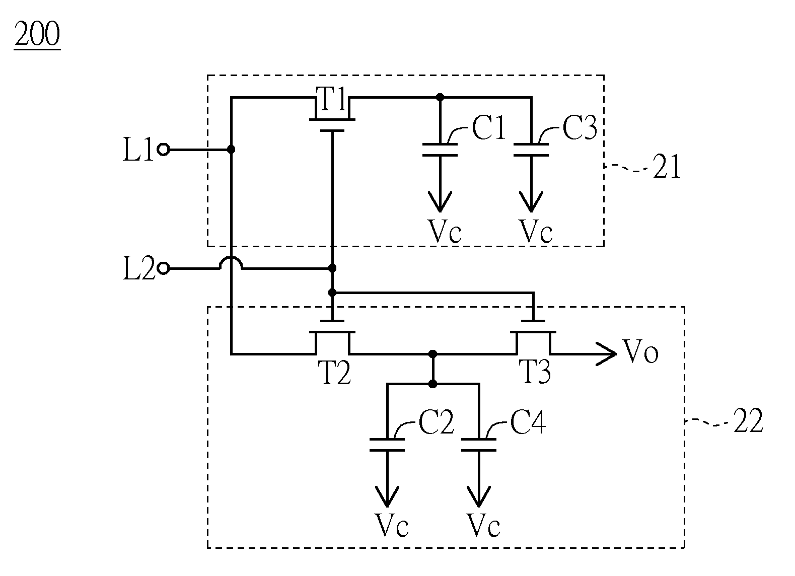
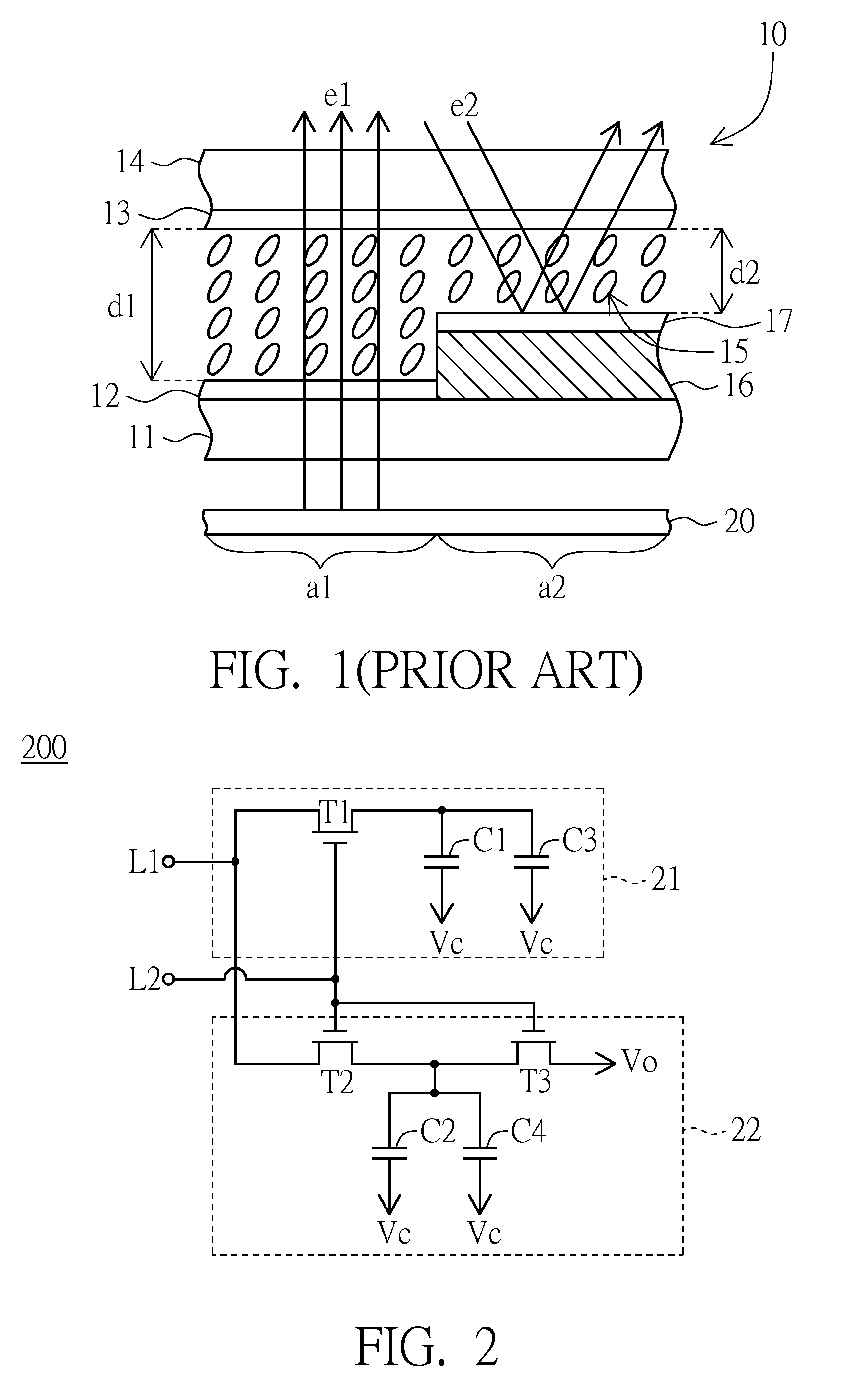
[0018]The pixel circuit structure according to the present embodiment is applied in an LCD panel which includes many scan lines, many data lines and many pixel units, wherein each pixel unit preferably includes one pixel circuit structure of the present embodiment. The following elaboration will be made in accordance with a single pixel circuit structure, so as to clearly show the characteristics of the pixel circuit structure according to the present embodiment.

[0019]Referring to FIG. 2, a perspective view of the pixel circuit structure according to the first embodiment of the invention is shown. The LCD panel adopting the pixel circuit structure 200 according to the present embodiment has a common voltage Vc and includes at least one data line L1. The pixel circuit structure 200 includes a first circuit 21 and a second circuit 22. The first circuit 21 includes a first switch T1 and a first capacitor C1. One end of the capacitor receives the common voltage Vc. Two ends of the first...

second embodiment

[0027]Referring to FIG. 4, a perspective view of a pixel circuit structure according to the second embodiment of the invention is illustrated. As shown in FIG. 4, the pixel circuit structure 400 of the present embodiment is different from the above-described pixel circuit structure 200 of the first embodiment in the manner of how the second switch T2 is coupled to the data line L1 and therefore similarities between them will not be repeated for the sake of brevity hereinafter. In addition, same designations in the figures denote similar elements of the embodiments. The pixel circuit structure 400 is suitable for use in an LCD panel. The LCD panel has a common voltage Vc and includes at least one data line L1. The pixel circuit structure 400 includes a first circuit 41 and a second circuit 42. The first circuit 41 includes a first capacitor C1 and a first switch T1. The second circuit 42 includes a second switch T2, a third switch T3 and a second capacitor C2. One end of the first ca...


PUM

PropertyMeasurementUnit
voltagesaaaaaaaaaa
voltagesaaaaaaaaaa
voltageaaaaaaaaaa

Abstract

A pixel circuit structure applied in an LCD panel, which has a common voltage and includes at least one data line, is provided. The pixel circuit structure includes a first and a second circuit. The first circuit includes a first switch and a first capacitor. The second circuit includes a second switch, a third switch and a second capacitor. One end of the first capacitor receives the common voltage. Two ends of the first switch are respectively coupled to the data line and the other end of the first capacitor. The second and the third switch are coupled serially between the data line and a voltage source. One end of the second capacitor receives the common voltage, and the other end is coupled between the second and the third switch. The potential difference between the two ends of the first capacitor is different from that of the second capacitor.

Description

[0001]This application claims the benefit of Taiwan application Serial No. 96137570, filed Oct. 5, 2007, the subject matter of which is incorporated herein by reference.BACKGROUND OF THE INVENTION[0002]1. Field of the Invention[0003]The invention relates in general to a pixel circuit structure, and more particularly to a pixel circuit structure applied in a liquid crystal display panel.[0004]2. Description of the Related Art[0005]The consumption market of consumer electronic products, such as personal digital assistants (PDAs), mobile phones, laptops, projectors, and even large-size flat panel televisions, expands rapidly in recent years, and therefore facilitates the increment of the quantity demanded for liquid crystal display (LCD) panel. Further, along with the maturity of the market and the progress of the technology, consumers are demanding for higher and higher display quality of LCD panels.[0006]Referring to FIG. 1, a perspective of a single pixel in a conventional transflec...

Claims


Application Information

Patent Timeline
Patent Type & Authority Applications(United States)
IPC IPC(8): G02F1/133
CPCG09G3/3614G09G3/3648G09G2320/028G09G2300/0447G09G2300/0456G09G2300/0443
Inventor TSAI, YI-CHENGWANG, I-FANGWANG, WEN-CHUNKANG, HEN-TAKUO, KAI-LUNYU, MING-CHANGTSAI, WAN-JEN
Owner WINTEK CORP
Why Eureka
Try Eureka