Pixel electrode and array substrate

A technology of pixel electrodes and array substrates, applied in nonlinear optics, instruments, optics, etc., can solve the problems of small line width and line spacing of pixel electrodes, achieve the effect of reducing energy consumption and improving liquid crystal efficiency

Inactive Publication Date: 2019-02-22
SHENZHEN CHINA STAR OPTOELECTRONICS SEMICON DISPLAY TECH CO LTD
View PDF5 Cites 4 Cited by
  • Summary
  • Abstract
  • Description
  • Claims
  • Application Information

AI Technical Summary

Problems solved by technology

[0006] The present application provides a pixel electrode and an array substrate to solve the technical problem that the line width and line spacing of the existing pixel electrodes are small

Method used


Image

  • Pixel electrode and array substrate
  • Pixel electrode and array substrate
  • Pixel electrode and array substrate

Examples


Embodiment Construction

[0029] The following descriptions of the various embodiments refer to the accompanying drawings to illustrate specific embodiments that the present application can be used to implement. The directional terms mentioned in this application, such as [top], [bottom], [front], [back], [left], [right], [inside], [outside], [side], etc., are for reference only The orientation of the attached schema. Therefore, the directional terms used are used to illustrate and understand the application, but not to limit the application. In the figures, structurally similar elements are denoted by the same reference numerals.

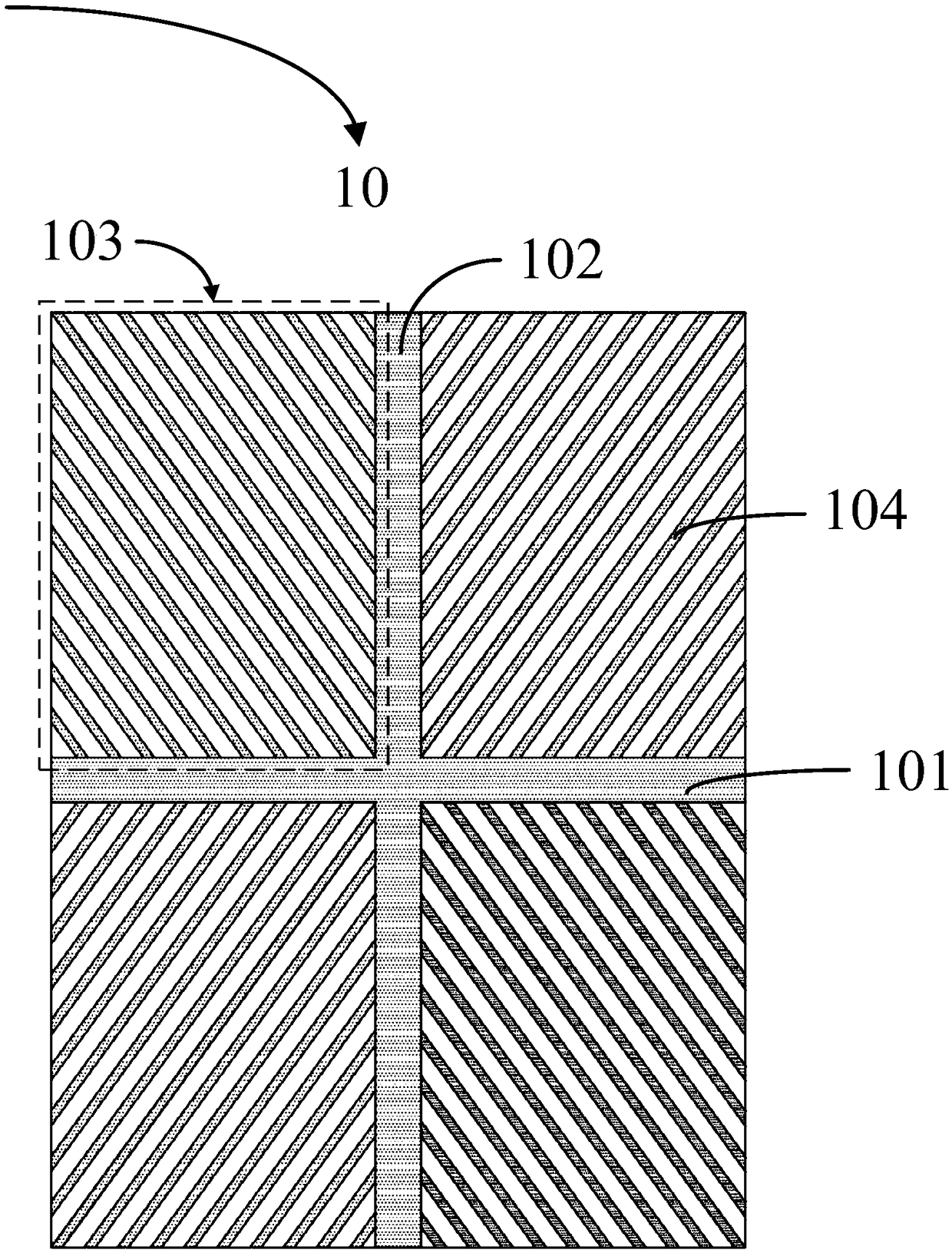
[0030] see figure 1 , figure 1 It is a structural diagram of the pixel electrode of the present application.

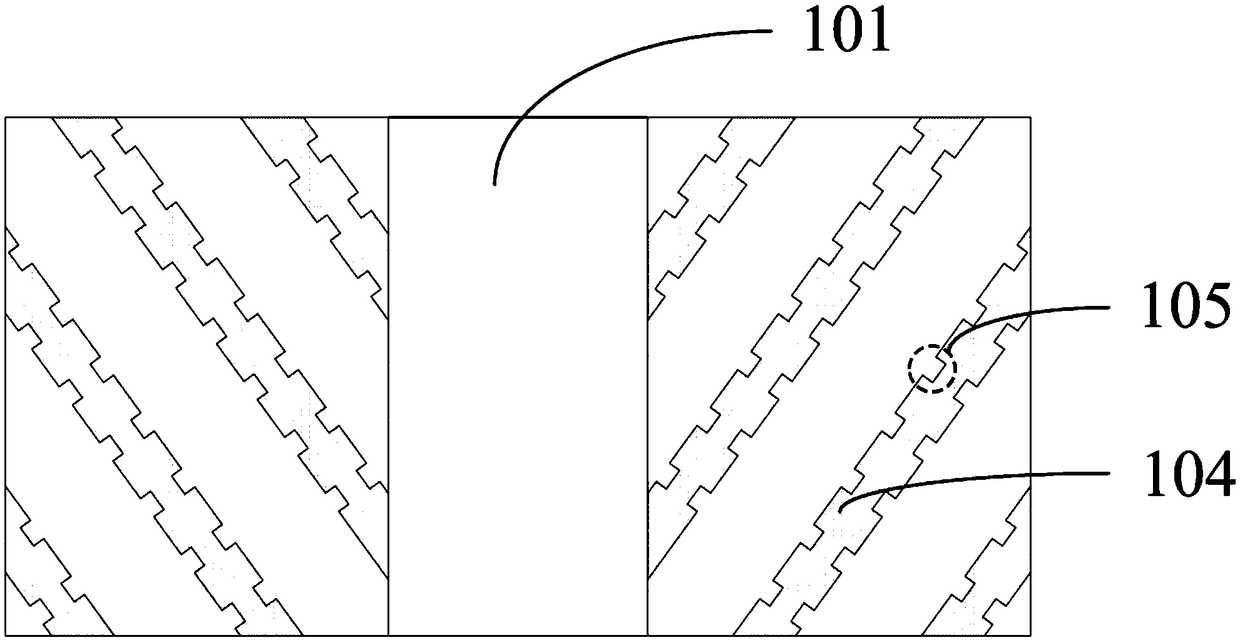
[0031] see figure 2 , figure 2 It is a partially enlarged view of the pixel electrode of this application.

[0032] The pixel electrode 10 includes a first main electrode 101 and a second main electrode 102 vertically intersecting the first main electrode ...


PUM

PropertyMeasurementUnit
angleaaaaaaaaaa

Abstract

The invention provides a pixel electrode and an array substrate. The pixel electrode comprises a first main electrode and a second main electrode which is vertically intersected with the first main electrode; the first main electrode and the second main electrode divide the pixel electrode into a plurality of liquid crystal alignment areas, a plurality of branch electrodes are arranged in each liquid crystal alignment area, and a preset included angle is formed between each branch electrode and the first main electrode or the second main electrode, wherein each branch electrode is provided with a hollowed-out part. According to the pixel electrode, the hollowed-out parts are arranged on the branch electrodes of the pixel electrode, so that the wire width of the branch electrodes is reduced, and the wire distance between every two adjacent branch electrodes is increased in order to improve the liquid crystal efficiency in a liquid crystal displayer and lower the energy consumption of the displayer.

Description

technical field [0001] The present application relates to the display field, in particular to a pixel electrode and an array substrate. Background technique [0002] Liquid crystal display (Liquid Crystal Display, LCD) is currently the most widely used display product in the market. Its production process technology is very mature, the product yield rate is high, the production cost is relatively low, and the market acceptance is high. [0003] Currently, conventional liquid crystal displays include an array substrate, a color filter substrate, and a liquid crystal layer located between the array substrate and the color filter substrate. Pixel electrodes are arranged on the side of the array substrate, and common electrodes are arranged on the side of the color filter substrate. The liquid crystal display drives the liquid crystal to deflect through the voltage difference between the pixel electrode and the common electrode, so that the liquid crystal display displays image...

Claims


Application Information

Patent Timeline
Patent Type & Authority Applications(China)
IPC IPC(8): G02F1/1343
CPCG02F1/134309G02F1/134345
Inventor 郝思坤
Owner SHENZHEN CHINA STAR OPTOELECTRONICS SEMICON DISPLAY TECH CO LTD
Why Eureka
Try Eureka