

Manufacturing method for touch panel edge wire routing, touch panel and touch display device
A technology of edge routing and touch panel, applied in chemical/electrolytic methods to remove conductive materials, input/output process of data processing, instruments, etc., can solve problems affecting signal output results, signal errors, signal interference, etc. , to achieve the effect of large touch area and display area, good bad or wrong signal, and avoiding bad situations
- Summary
- Abstract
- Description
- Claims
- Application Information
AI Technical Summary
Problems solved by technology
Method used
Image

Examples
Embodiment Construction
[0054] Below in conjunction with accompanying drawing and embodiment the present invention is described in detail:
[0055] Before the present invention is described in detail, it should be noted that in the following description, similar elements are denoted by the same reference numerals.
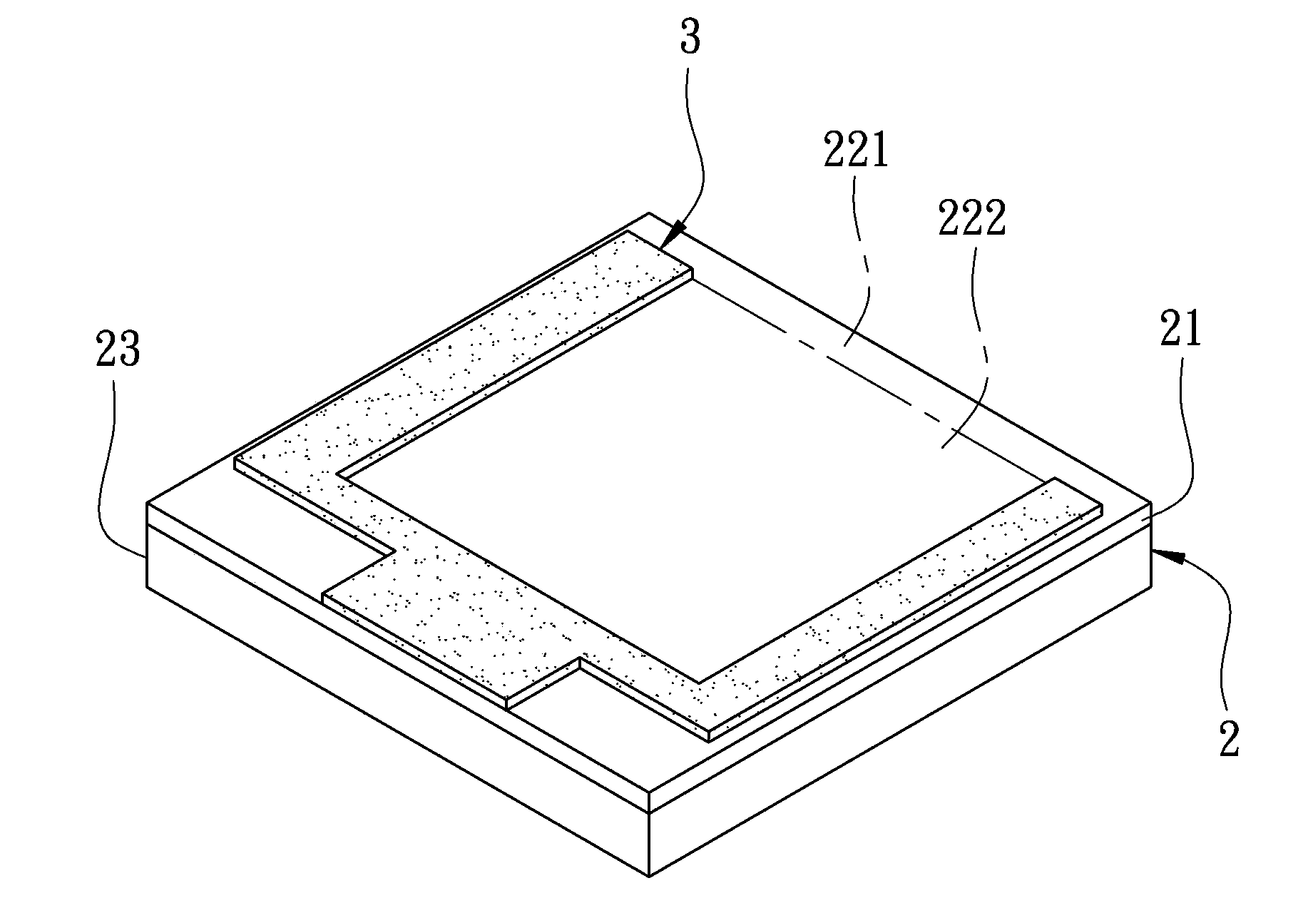
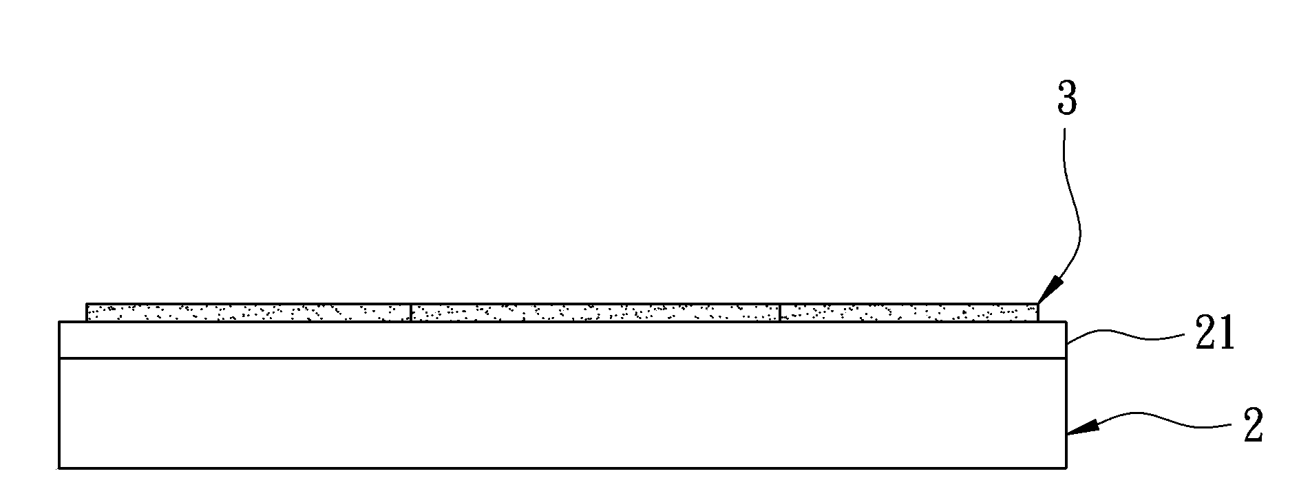
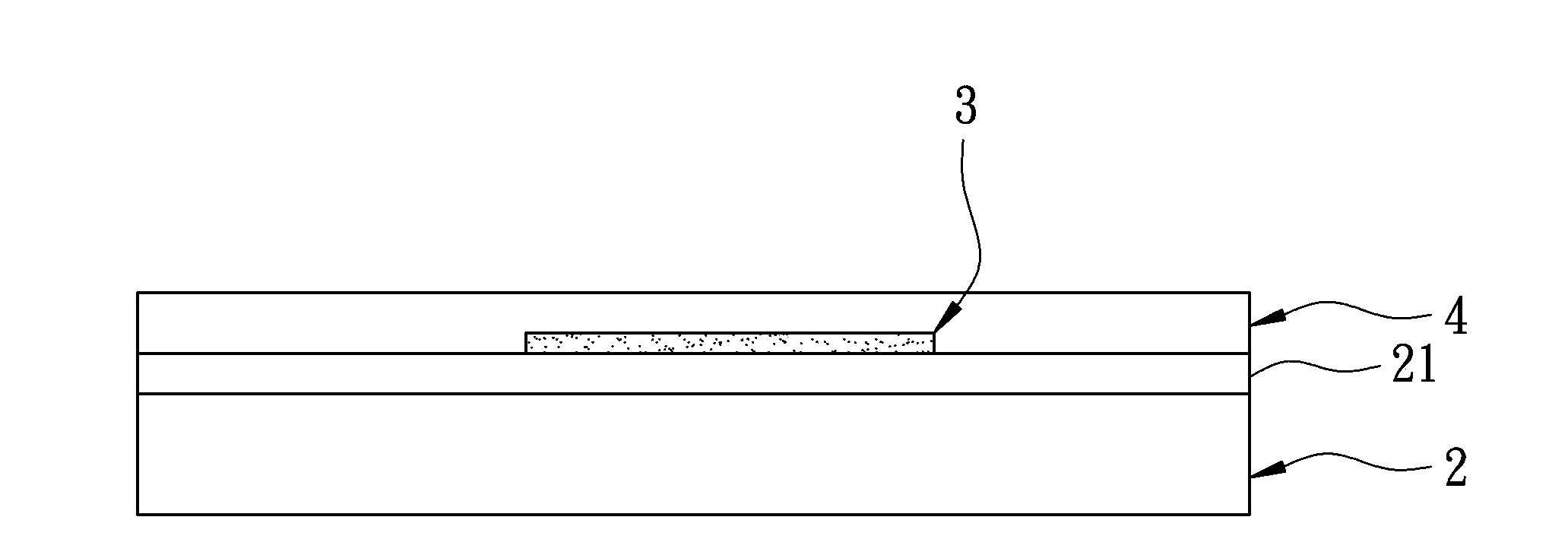
[0056] refer to Figure 1 to Figure 10 , illustrating the continuous steps of a first preferred embodiment of the method for manufacturing the edge traces of the touch panel of the present invention, wherein, figure 2 and image 3 are from figure 1 Schematic diagram of the side view taken from the front. The preparation method comprises the following steps:
[0057] refer to figure 1 , figure 2 and image 3 , the step (a) is to form a layer of photosensitive conductive paste layer 3 on an edge region 221 of a base material 2 with a layer of transparent conductive layer 21, and make the photosensitive conductive paste layer 3 at least in contact with the transparent conductive lay...
PUM
| Property | Measurement | Unit |
|---|---|---|
| Viscosity | aaaaa | aaaaa |
| Thickness | aaaaa | aaaaa |
| Particle size | aaaaa | aaaaa |
Abstract
Description
Claims
Application Information