Dual mosaic structure, interconnect structure and methods for fabricating the same

A technology of dual damascene structure and internal connection structure, which is applied in semiconductor/solid-state device manufacturing, electrical components, electric solid-state devices, etc., and can solve problems affecting the reliability of integrated circuit devices, peeling, and forming holes

Active Publication Date: 2008-07-16
TAIWAN SEMICON MFG CO LTD
View PDF7 Cites 0 Cited by
  • Summary
  • Abstract
  • Description
  • Claims
  • Application Information

AI Technical Summary

Problems solved by technology

If such tensile stress continues to accumulate in the semiconductor structure, it will cause deformation (deformation) or bending (bowing), cracking (cracking), peeling (peeling) or holes in the inner film layer of the overall semiconductor structure, thus destroying It affects the interconnection structure including these film layers and affects the reliability of the integrated circuit device formed by it.
Based on the above reasons, low dielectric constant dielectric materials are more difficult to integrate into existing integrated circuit structures and manufacturing processes than traditional silicon dioxide materials. Therefore, when integrated circuit devices and their manufacturing processes use low dielectric constant to replace traditional The above problems may occur when the silica material

Method used


Image

  • Dual mosaic structure, interconnect structure and methods for fabricating the same
  • Dual mosaic structure, interconnect structure and methods for fabricating the same
  • Dual mosaic structure, interconnect structure and methods for fabricating the same

Examples


Embodiment Construction

[0038] Hereinafter, the description "low dielectric constant" is used to indicate a lower dielectric constant than that of conventional silicon dioxide. Preferably, low dielectric constant refers to a dielectric constant lower than 4.

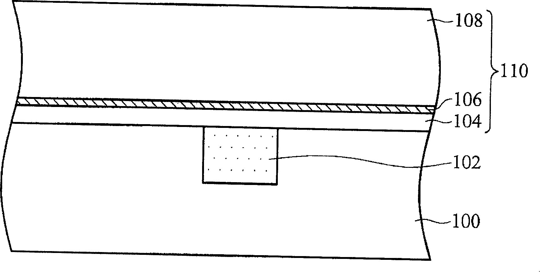
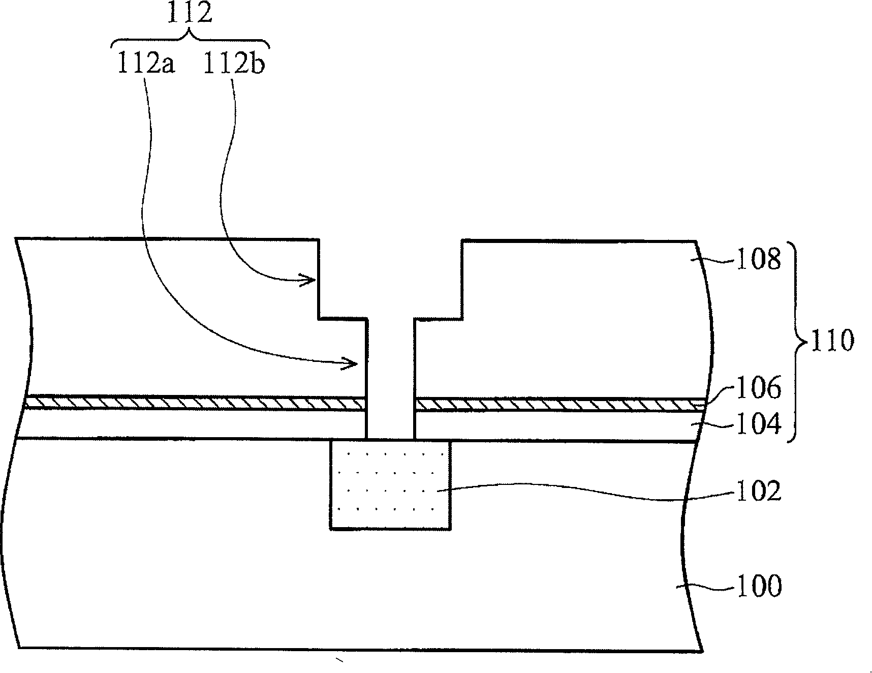
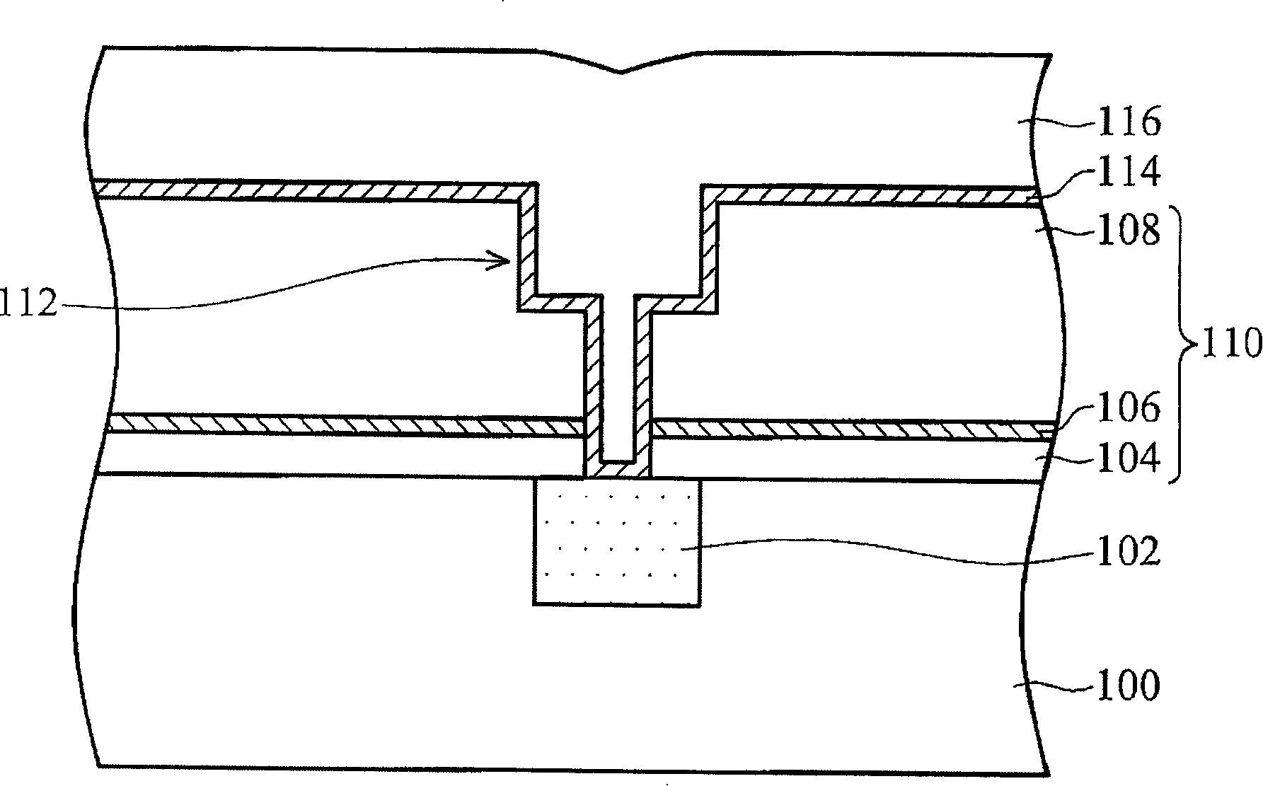
[0039] Embodiments of the interconnect structure and method of manufacture of the present invention will cooperate with Figure 1 to Figure 4 Describe in detail as follows. Please refer to figure 1 As shown, a semiconductor substrate is provided on which semiconductor devices and other conductive structures are disposed. To simplify the drawing, a flat substrate 100 is shown here. In addition, if figure 1 As shown, a conductive member 102 is formed in the substrate 100, which may be electrically coupled to a semiconductor device or a wire (not shown) therebelow.

[0040] Next, the low-k dielectric layers 104 , 108 with the first stress type and the stress adjustment layer 106 with the second stress type are alternately formed on the subs...


PUM

PropertyMeasurementUnit
thicknessaaaaaaaaaa

Abstract

The present invention relates to interconnects with harmonized stress and methods for fabricating the same. An interconnect comprises a substrate having a conductive member. A composite low-k dielectric layer interposed with at least one stress-harmonizing layer therein overlies the substrate. A conductive feature in the composite low-k dielectric layer passes through the at least one stress-harmonizing layer to electrically connect the conductive member.

Description

technical field [0001] The present invention relates to semiconductor devices, and more particularly to an interconnect structure in an integrated circuit. Background technique [0002] As the size of integrated circuit devices shrinks, the arrangement of conductive interconnects such as metal wires within the integrated circuit device becomes closer and the horizontal spacing between them is further reduced. In this way, the capacitance of the structure between the conductive interconnects increases, which causes RC delay time and crosstalk effect. In order to solve the above problems, the traditional silicon dioxide material (dielectric constant is about 4) has been replaced by a dielectric material with a low dielectric constant in today's interconnect manufacturing technology, so as to reduce the capacitance of the structure between conductive interconnects value. [0003] Compared with traditional silicon dioxide materials, most low-k dielectric materials exhibit high...

Claims


Application Information

Patent Timeline
Patent Type & Authority Patents(China)
IPC IPC(8): H01L21/768H01L23/522
CPCH01L23/53295H01L21/76801H01L21/76829H01L21/76835H01L21/76807H01L2924/0002H01L2924/00H01L21/28H01L21/3205
Inventor 卢永诚蔡明兴
Owner TAIWAN SEMICON MFG CO LTD
Why Eureka
Try Eureka