Semiconductor memory device and method of arranging signal and power lines thereof

a technology of semiconductor memory and signal, applied in the direction of information storage, static storage, digital storage, etc., can solve the problems of reducing power supply stability, reducing power supply width, and increasing voltage drop and power consumption, so as to reduce power line width, and reduce power line width

Active Publication Date: 2007-01-09
SAMSUNG ELECTRONICS CO LTD
View PDF17 Cites 18 Cited by
  • Summary
  • Abstract
  • Description
  • Claims
  • Application Information

AI Technical Summary

Benefits of technology

[0018]As DRAM devices scale to smaller cell dimensions and / or increase the number of cells in a memory array, more signal lines are routed over the memory array and row decoder per unit area in essentially the same area that previously served a smaller number of signal lines. The width of the power lines is therefore decreased proportionally to accommodate the denser array. Decreasing power line width is undesirable, however, as decreased power line width results in greater resistance to current flow, greater voltage drop and power consumption, and reduced power supply stability as current demands fluctuate. The various signal and power lines are also packed closer together as the device scales to smaller dimensions, resulting in an undesirable crosstalk between adjacent lines.
[0019]The embodiments described herein adopt a triple-metal-layer DRAM design that improves signal and power line routing considerably as opposed to a dual-metal-layer design. Although others have proposed various schemes to route signals over a memory array using three metal layers, it is believed that the present design addresses the problem with particular attention to the power supply issue, and thus produces a group of novel metal layer arrangements that scale well to smaller cell sizes.

Problems solved by technology

Decreasing power line width is undesirable, however, as decreased power line width results in greater resistance to current flow, greater voltage drop and power consumption, and reduced power supply stability as current demands fluctuate.
The various signal and power lines are also packed closer together as the device scales to smaller dimensions, resulting in an undesirable crosstalk between adjacent lines.

Method used


Image

  • Semiconductor memory device and method of arranging signal and power lines thereof
  • Semiconductor memory device and method of arranging signal and power lines thereof
  • Semiconductor memory device and method of arranging signal and power lines thereof

Examples


first embodiment

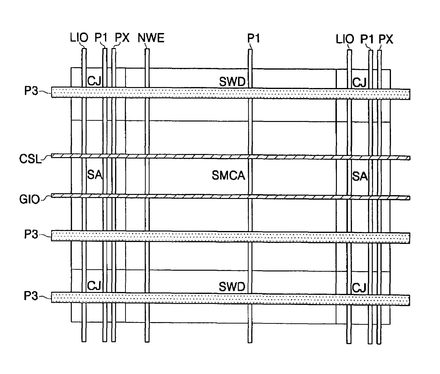
[0029]FIG. 6 illustrates a first embodiment with signal and power lines routed over a memory array using three layers of metal. The first metal layer contains NWE, PX, LIO signal lines and P1 power lines, similar to the prior art. The second metal layer contains CSL and GIO signal lines, and no power lines. The third metal layer contains power lines P3 perpendicular to the P1 power lines formed with the first metal layer. The P3 power lines can be made wider than the prior art P2 power lines formed with the second metal layer because the CSL and GIO lines do not compete for the metal 3 area overlying the memory array. Although for purposes of clarity the feature is not illustrated in FIG. 6, portions of the P3 lines can even directly overlie CSL and GIO lines. Connections to power lines P1 exist in clearances where a P3 line overlies a P1 line of the same voltage, and may use a via contact (direct connection between the third metal and the first metal) or intermediate P2 pad (not sh...

second embodiment

[0030]FIG. 7 illustrates a second embodiment with signal and power lines routed over a memory array using three layers of metal. In this embodiment, P1 lines do not exist on metal 1, and P2 lines parallel to CSL and GIO on metal 2 distribute power to the memory array circuitry. P3 lines are arranged on metal 3, perpendicular to the P2 lines and connecting to the P2 lines where a P3 line and a P2 line of the same voltage level cross. The P2 lines can remain relatively thin, while the P3 lines can be made relatively wide to efficiently carry current to the vicinity where it will be needed.

third embodiment

[0031]FIG. 8 illustrates a third embodiment with signal and power lines routed over a memory array using three layers of metal. In this embodiment, thin P1 power lines are crossed by thin P2 power lines. P1 and P2 lines of the same voltage level connect where they cross. Wider P3 power lines are routed parallel to the P2 lines, and generally overlap the P2 lines of the same voltage level. As the P3 and P2 lines overlap along their length, connection between the two lines can be made in long channels or in more frequent, abbreviated vias. The P3 / P2 structures have lower resistance per unit length while occupying far less space on the metal layer shared with CSL and GIO.


PUM


Abstract

Method and apparatus for use, e.g., with Synchronous Dynamic Random Access Memory (SDRAM) circuits are disclosed. In one described embodiment, three metal layers are deposited and patterned in turn overlying a memory array portion of an SDRAM. Relatively wide power conductors are routed on a third metal layer, allowing power conductors to be reduced in size, or in some cases eliminated, on first and second metal layers. The relatively wide power conductors thus can provide a more stable power supply to the memory array, and also free some space on first and / or second metal for routing of additional and / or more widely spaced signal conductors. Other embodiments are described and claimed.

Description

BACKGROUND OF THE INVENTIONRELATED APPLICATIONS [0001]This application claims the benefit of priority to Korean Patent Applications P2004-40542, filed Jun. 3, 2004, and P2004-74730, filed Sep. 17, 2004, the disclosures of which are incorporated herein by reference.[0002]1. Field of the Invention[0003]The present invention relates to dynamic random access memory (DRAM) semiconductor devices, and more particularly to methods and apparatus for routing power and signal traces in patterned metal layers overlying such devices.[0004]2. Description of the Related Art[0005]DRAM devices include a memory array, circuitry to access the memory array, and peripheral circuitry to control DRAM operation and communicate with external devices. Typical memory arrays are formed of a repeating pattern of sub memory cell arrays interspersed with a portion of the circuitry used to access the memory array. The remainder of the access circuitry is generally located in a row decoder and a column decoder loca...

Claims


Application Information

Patent Timeline
Patent Type & Authority Patents(United States)
IPC IPC(8): G11C5/06G11C5/14G11C11/4074
CPCG11C5/063G11C11/4074G11C5/14
Inventor LEE, JAE-YOUNGKWON, JOON-HYUKKIM, CHI-WOOKKIM, SUNG-HOONPARK, YOUN-SIK
Owner SAMSUNG ELECTRONICS CO LTD
Why Eureka
Try Eureka