Nanocircuit and self-correcting etching method for fabricating same

a technology of nanocircuits and etching methods, applied in the field of microstructures, can solve the problems of high variation in cd and substantial increase in power dissipation, and achieve the effect of reducing line width variation and reducing line width

Inactive Publication Date: 2006-04-11
INT BUSINESS MASCH CORP
View PDF3 Cites 21 Cited by
  • Summary
  • Abstract
  • Description
  • Claims
  • Application Information

AI Technical Summary

Benefits of technology

[0013]These and other objects and advantages are achieved in the present invention by utilizing a self-correcting etching (SCORE) process. The SCORE process of the present invention is particularly useful for reducing preselected features of a hard mask without degrading the variation of the critical dimension (CD) within each wafer. Alternatively, the CD variation of the hard mask features' produced during printing can be substantially reduced by applying SCORE. Hence, ultra-sub-lithographic features (e.g., nanostructures) can be reliably fabricated. Consequently, the method of the present invention can be used to increase the circuit performance, while improving the manufacturing yield and reducing power consumption.
[0021]performing a self-correcting dopant-sensitive etching process on a plurality of exposed patterned multi-layered stacks to provide patterned lines that have a substantially reduced line width and substantially reduced line width variation; and

Problems solved by technology

Such a high variation in CD is unwanted since it does not permit reliable fabrication of ultra-sub-lithographic features.
Additionally, the high variation in CD is unwanted since it hinders device performance and manufacturing yield and results in a substantial increase of power dissipation.

Method used


Image

  • Nanocircuit and self-correcting etching method for fabricating same
  • Nanocircuit and self-correcting etching method for fabricating same
  • Nanocircuit and self-correcting etching method for fabricating same

Examples


Embodiment Construction

[0036]The present invention, which provides a method of fabricating structures having ultra-sub-lithographic features (less than 0.7 F) and the resultant structures formed therefrom, will now be described in greater detail by referring to the drawings that accompany the present application. In the accompanying drawings, like and corresponding elements are referred to by like reference numerals.

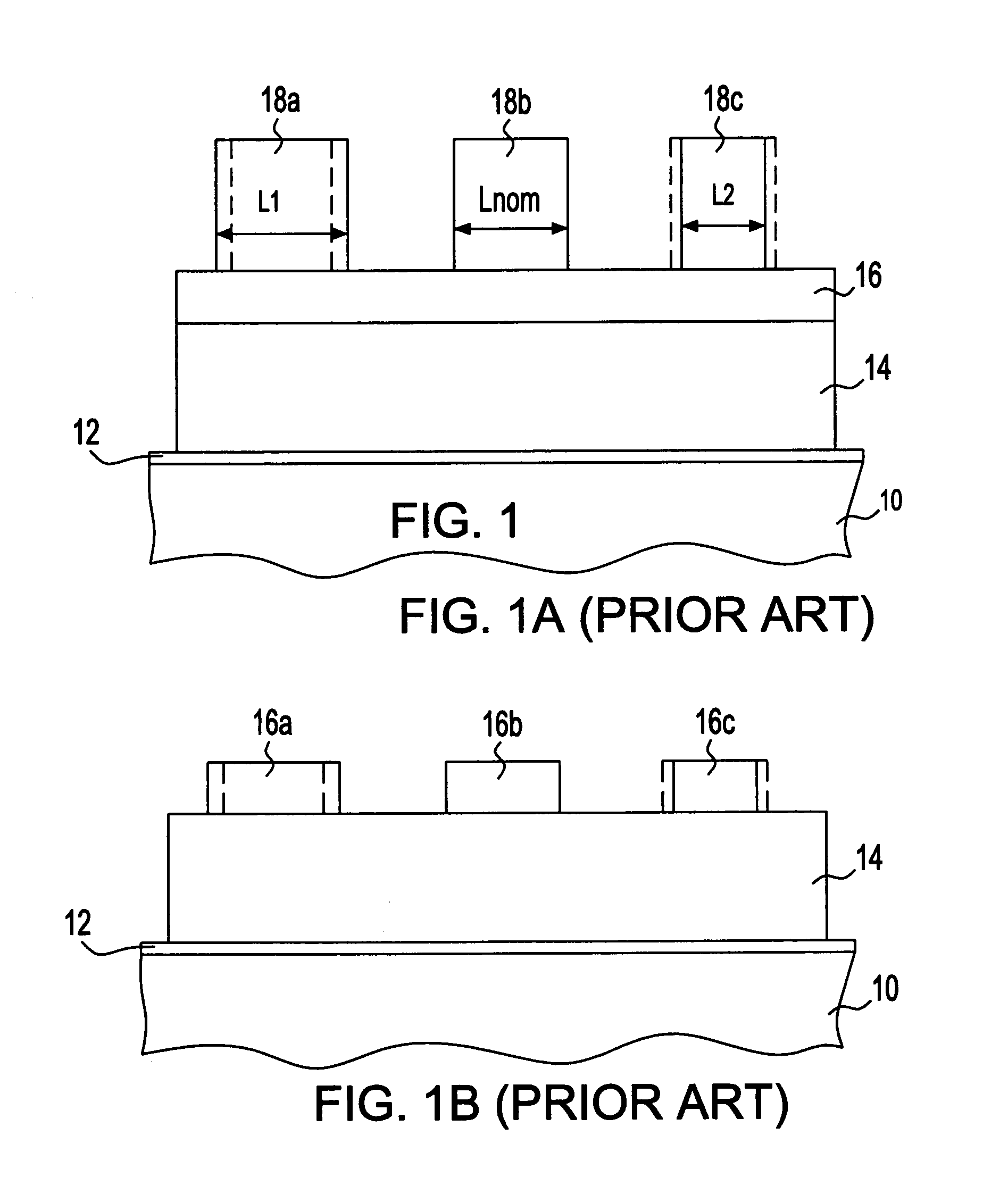
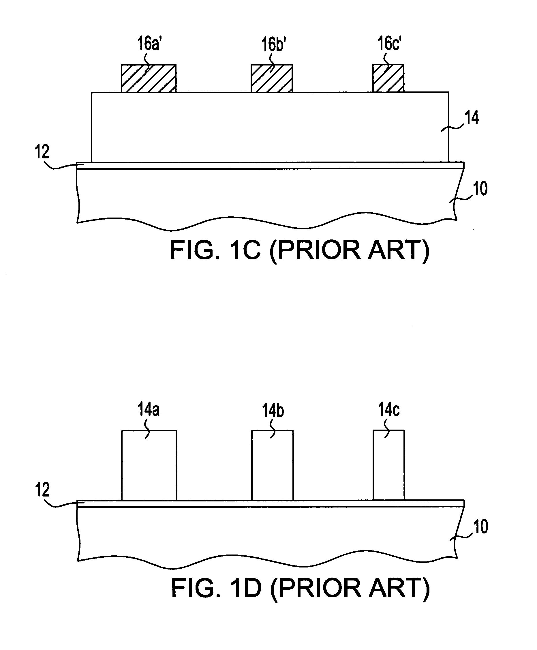
[0037]Referring to FIGS. 3A–3J, there is shown one possible implementation of the present invention for fabricating gate microstructures. Although the drawings and description that follow are specific for the formation of gate microstructures, the present invention may be used in fabricating any microstructure provided that the microstructure includes at least one etchable material.

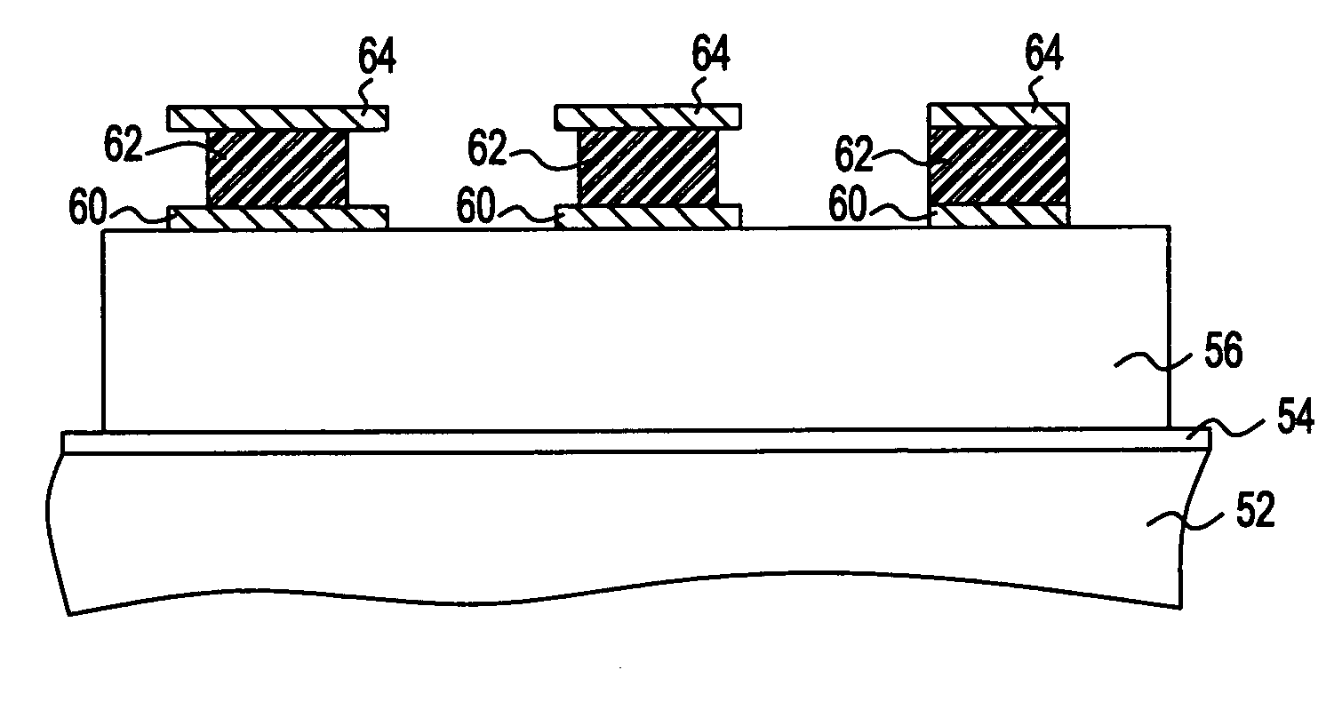
[0038]Referring to FIG. 3A, there is shown an initial structure 50 that may be employed in the present invention. The initial structure 50 includes a semiconductor substrate 52, a gate dielectric 54 located on a sur...


PUM

PropertyMeasurementUnit
temperatureaaaaaaaaaa
thicknessaaaaaaaaaa
thicknessaaaaaaaaaa

Abstract

A self-correcting etching (SCORE) process for fabricating microstructure is provided. The SCORE process of the present invention is particularly useful for reducing preselected features of a hard mask without degrading the variation of the critical dimension (CD) within each wafer. Alternatively, the CD variation of the hard mask features' produced during printing can be substantially reduced by applying SCORE. Hence, ultra-sub-lithographic features (e.g., nanostructures) can be reliably fabricated. Consequently, the method of the present invention can be used to increase the circuit performance, while improving the manufacturing yield.

Description

FIELD OF THE INVENTION[0001]The present invention relates to microstructures, including nanostructures and nanocircuits, and a method of fabricating the same. More particularly, the present invention relates to a method for self-correcting etching (SCORE) of various microstructures.BACKGROUND OF THE INVENTION[0002]In the field of semiconductor device manufacturing, there is a need for providing semiconductor devices such as complementary metal oxide semiconductor (CMOS) devices that contain ultra-sub-lithographic features. That is, there is a need for providing CMOS lines in which the dimensions thereof are less than 0.7 F, wherein F is the minimal lithographic dimension related to the wavelength of exposure.[0003]In the prior art, CMOS devices that have a gate microstructure are fabricated using photolithography, which includes the steps of applying a photoresist and an optional antireflective coating (ARC) to a material needing patterning; exposing the photoresist to a pattern of ...

Claims


Application Information

Patent Timeline
Patent Type & Authority Patents(United States)
IPC IPC(8): H01L21/461H01L21/033H01L21/302H01L21/3205H01L21/3213H01L21/8238H01L29/76H01L31/062
CPCH01L21/0332H01L21/0337H01L21/32139H01L21/82385H01L21/0338Y10S438/947
Inventor DOKUMACI, OMER H.GLUSCHENKOV, OLEG
Owner INT BUSINESS MASCH CORP
Why Eureka
Try Eureka