Ceramic capacitor and method of manufacturing same

a ceramic capacitor and capacitor technology, applied in the field of ceramic capacitors, can solve the problems of large changes in the thickness dimension of ceramic dielectric layers, difficult to precisely control this thickness dimension, and suffers in the conventional ceramic capacitor described above, so as to enhance the orientation stability of the internal electrode and increase the capacitance

Inactive Publication Date: 2010-08-05
HEADWAY TECH INC +1
View PDF10 Cites 3 Cited by
  • Summary
  • Abstract
  • Description
  • Claims
  • Application Information

AI Technical Summary

Benefits of technology

[0022]Further, the mode may also be such that an interdigitated branch part, which extends from one of the pair of internal electrodes toward the other one of the pair of internal electrodes, is formed on mutually opposing surfaces of the pair of internal electrodes. Since the areas of the opposing surfaces of the pair of internal electrodes are enlarged in accordance with this, increased capacitance is achieved. In addition to this, the orientation stability of the internal electrode is enhanced subsequent to removing the thick-film mask.

Problems solved by technology

However, the conventional ceramic capacitor described above suffers from the following problems.
That is, the manufacturing process comprises a process for pressure forming the stacked member of green sheets that constitutes the ceramic dielectric layers, and a process for baking this stacked member, thereby readily causing big changes to occur in the thickness dimensions of the ceramic dielectric layers, making it difficult to precisely control this thickness dimension.
That is, because it is not possible to precisely control the dimensions of the intervals between the internal electrode layers, variations in capacitance and other such device characteristics occur.

Method used


Image

  • Ceramic capacitor and method of manufacturing same
  • Ceramic capacitor and method of manufacturing same
  • Ceramic capacitor and method of manufacturing same

Examples


first embodiment

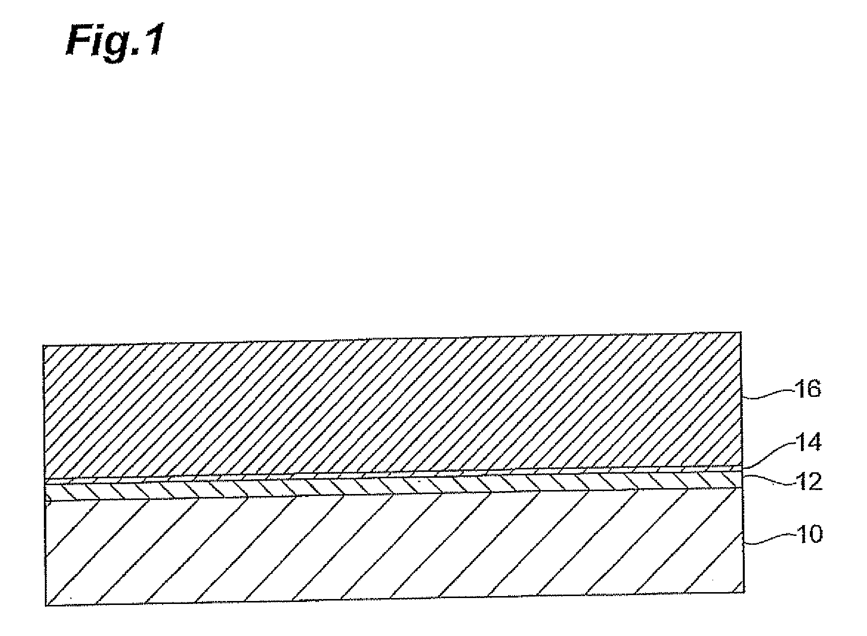
[0048]When manufacturing a ceramic capacitor related to the first embodiment of the present invention, first, as shown in FIG. 1, an Al2O3 insulation layer 12, Ni seed layer (first seed layer) 14, and thick-film photoresist masking layer 16 are sequentially stacked on top of a substrate 10 (for example, a silicon substrate). The seed layer 14 is 1000 Å thick, and the masking layer 16 is 6 μm thick.

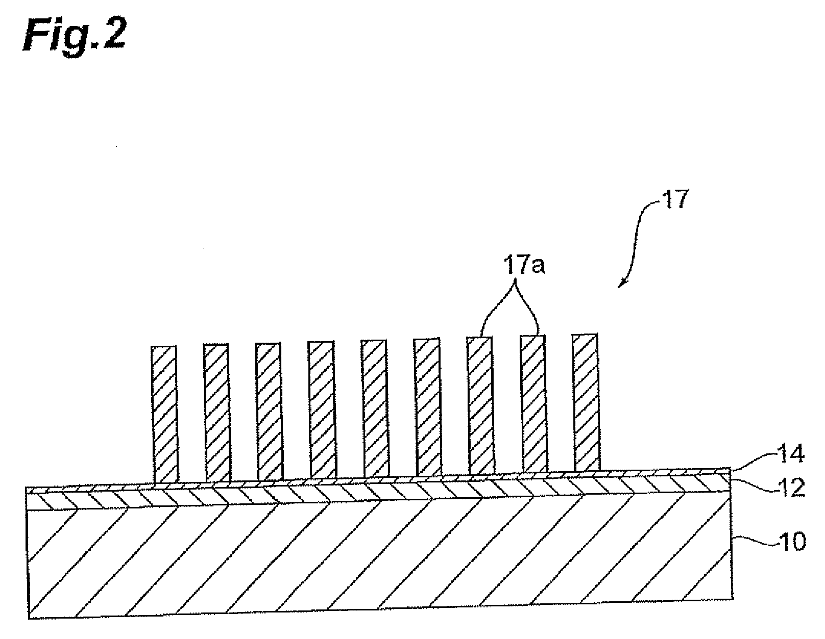
[0049]Next, as shown in FIG. 2, patterning of the masking layer 16 is carried out using a known photoresist technique to form a thick-film mask (first thick-film mask) 17. The thick-film mask 17 comprises a plurality of mask strips 17a between 0.4 and 0.6 μm wide extending perpendicularly relative to the surface of the substrate 10, and, for example, this plurality of mask strips 17a is arranged regularly at clearances of between 0.6 and 0.8 μm.

[0050]Then, as shown in FIG. 3, Ni plating of the seed layer 14 is carried out to form a plated layer 18A. This plated layer 18A is formed 5.5 μm t...

second embodiment

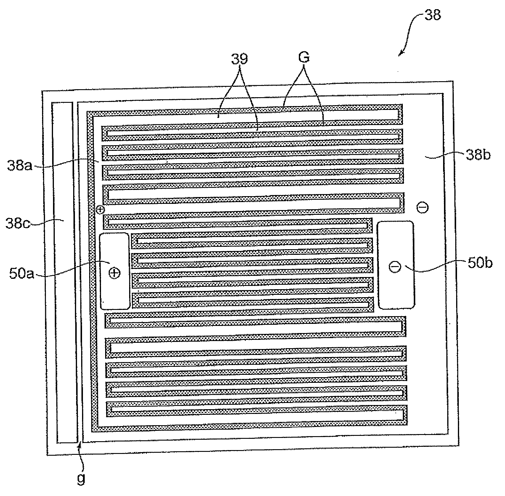
[0075]Next, a ceramic capacitor 1B related to a second embodiment of the present invention will be explained. This ceramic capacitor 1B, as shown in FIG. 13, constitutes a two-tiered ceramic capacitor comprising internal electrodes 18a, 18b, 18c in the first tier, and internal electrodes 38a, 38b, 38c in the second tier.

[0076]The steps for manufacturing the ceramic capacitor 1B will be explained below.

[0077]When manufacturing ceramic capacitor 1B, first, patterned internal electrodes 18a, 18b, 18c are formed on top of a substrate 10 in accordance with the same steps as those in the first embodiment. That is, subsequent to sequentially layering a Al2O3 insulation layer 12, a Ni seed layer (first seed layer) 14, and a thick-film photoresist masking layer 16 on top of the substrate 10, masking layer 16 patterning is carried out using a known photoresist technique to form a thick-film mask 17. Then, subsequent to carrying out the Ni plating of the seed layer 14 to form a plated layer 18...


PUM

PropertyMeasurementUnit
thickaaaaaaaaaa
thickaaaaaaaaaa
widthaaaaaaaaaa

Abstract

In a ceramic capacitor according to the present invention, an interdiginated pair of internal electrodes are arranged, on a substrate, perpendicular to a surface of the substrate, and a ceramic dielectric member is filled into a gap between this pair of internal electrodes. For this reason, the dimensions of the internal electrodes do not substantially change before and/or after the formation of the ceramic dielectric member, whereby the dimensions formed at the time of internal electrode can be maintained. According to this ceramic capacitor, since the internal electrode dimensions can be easily controlled like this, dimensional control of internal electrode spacing can also be easily carried out.

Description

BACKGROUND OF THE INVENTION[0001]1. Field of the Invention[0002]The present invention relates to a ceramic capacitor that is formed on a substrate, and a method of manufacturing same.[0003]2. Related Background Art[0004]In the past, a stacked ceramic capacitor has been known as one of ceramic capacitors. Such a stacked ceramic capacitor 1 has a structure as shown in FIG. 23, and is configured in accordance with a stacked member 6 in which some ceramic dielectric layers 2 and some internal electrode layers 4 are alternately stacked in a up-down direction, and a pair of electrodes 8A, 8B that are formed so as to sandwich this stacked member 6 laterally. Furthermore, regarding the internal electrode layers 4 of this capacitor 1, any two adjacent internal electrode layers 4 are connected to different electrodes 8A, 8B as shown FIG. 23B in detail.[0005]As a method of manufacturing the stacked ceramic capacitor described above, a sheet method and a print method are known. Both of these ma...

Claims


Application Information

Patent Timeline
Patent Type & Authority Applications(United States)
IPC IPC(8): H01G4/12
CPCH01G4/008H01G4/012Y10T29/435H01G4/232H01G4/30H01G4/12
Inventor SASAKI, YOSHITAKAIIJIMA, ATSUSHIIKEJIMA, HIROSHI
Owner HEADWAY TECH INC
Why Eureka
Try Eureka