Organic Light Emitting Diode Display Device

a light-emitting diode and display device technology, applied in the field of organic light-emitting diodes display devices, can solve the problems of low cost, inconvenient control method, and inability to fabricate large-sized or high-resolution panels, and achieve the effect of reducing motion artifacts

Active Publication Date: 2012-11-22
SAMSUNG DISPLAY CO LTD
View PDF8 Cites 34 Cited by
  • Summary
  • Abstract
  • Description
  • Claims
  • Application Information

AI Technical Summary

Benefits of technology

[0080]According to embodiments of the present invention, an OLED display device that can reduce motion artifact and assure light emission duration to be the maximum, and a display panel designed to be used in driving of the same are provided. For example, a display panel where pixel circuits are arranged to display a stereoscopic image without increasing frequency and design of the pixel circuits are provided. Accordingly, a large-sized display device having a large-sized display panel may be manufactured.

Problems solved by technology

The passive matrix type has a simple structure, thus the cost thereof is low; however, the passive matrix type is not suitable for fabricating large sized or high resolution panels.
However, its control method is technically more complicated and its cost is relatively high.
The driver having a high driving frequency may cause increase of production cost.
Moreover, as the display panel is increased in size and resolution, an RC delay of the display panel is increased so that the image data programming may not be efficiently performed.

Method used


Image

  • Organic Light Emitting Diode Display Device
  • Organic Light Emitting Diode Display Device
  • Organic Light Emitting Diode Display Device

Examples


Embodiment Construction

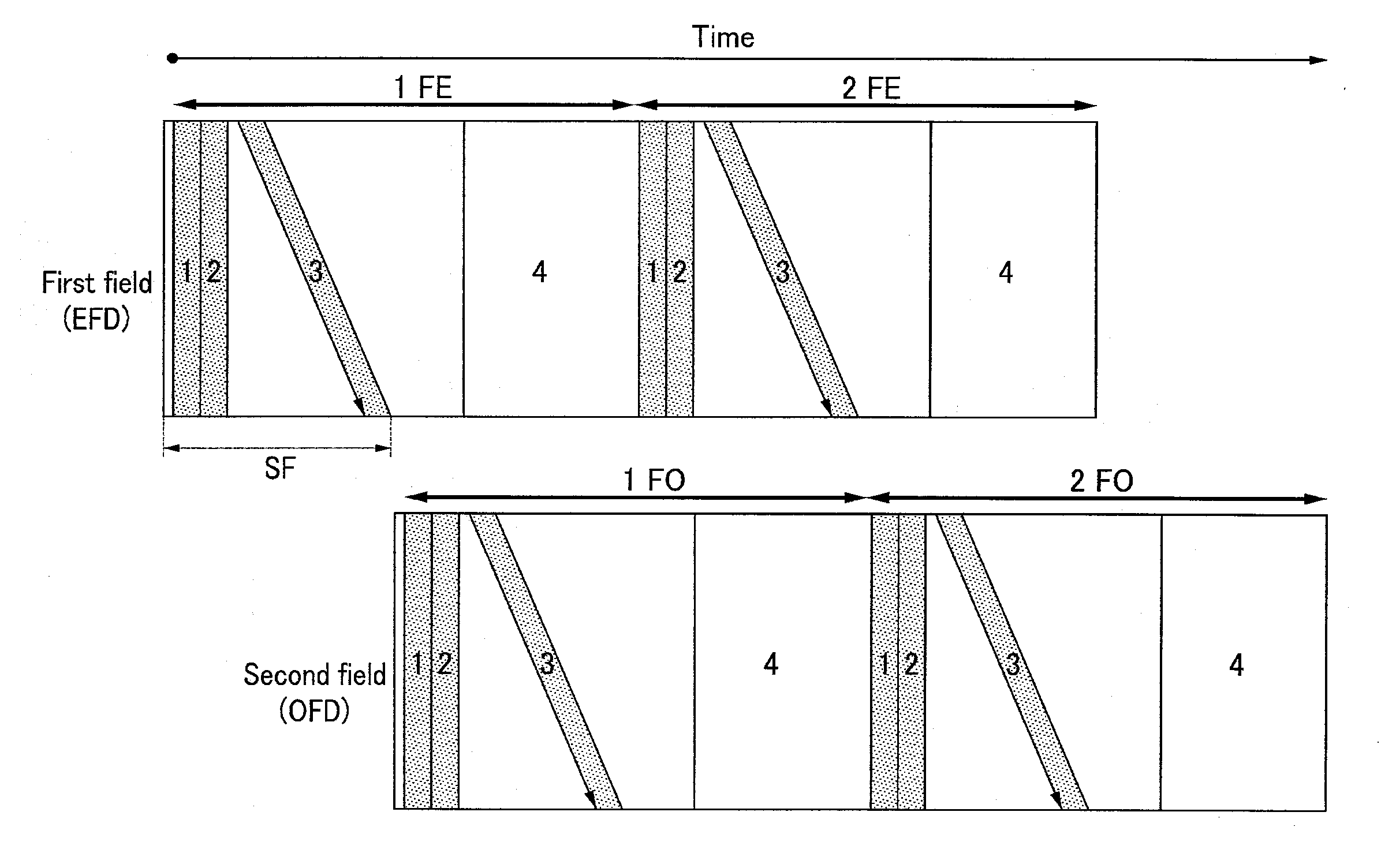
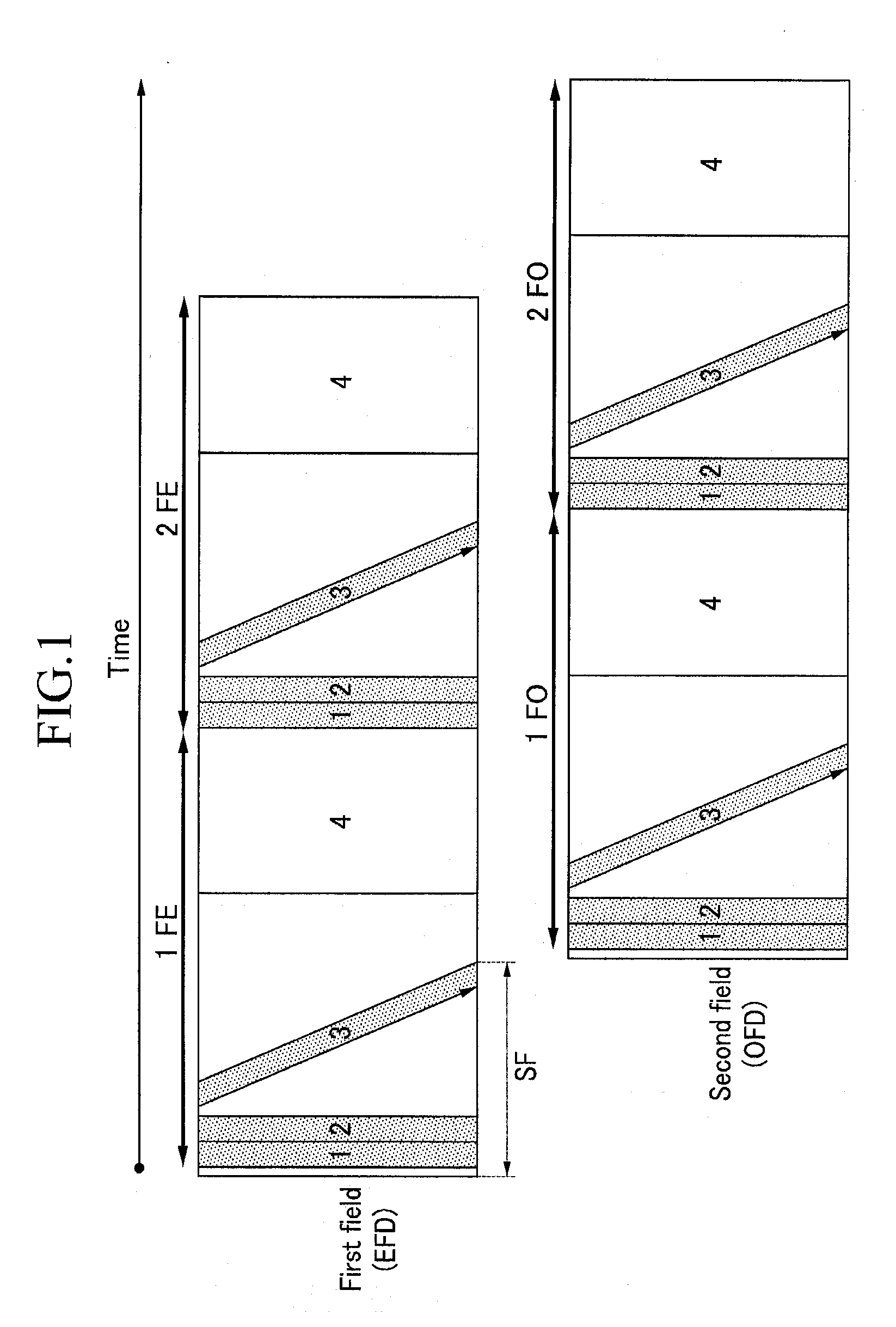
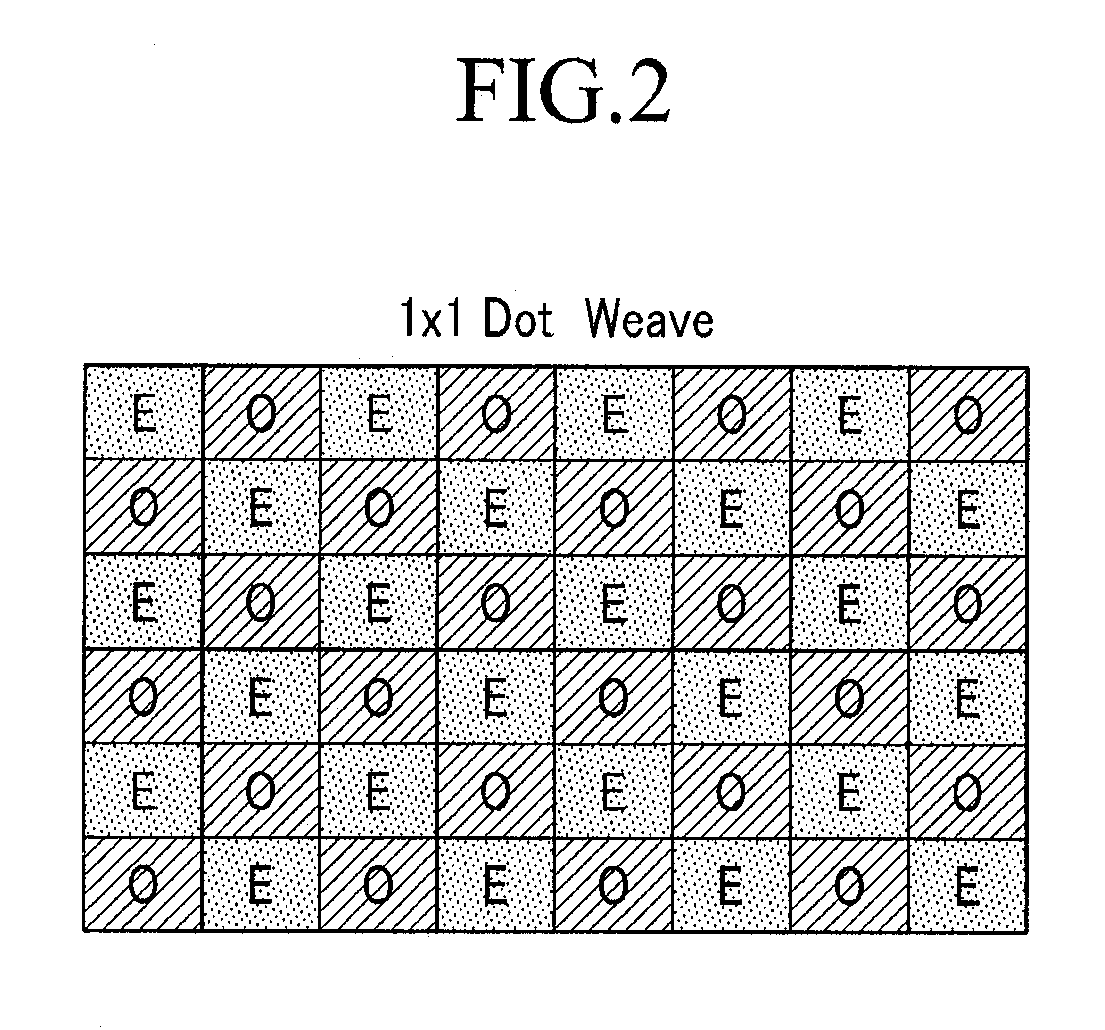
[0095]The present invention will be described more fully hereinafter with reference to the accompanying drawings, in which exemplary embodiments of the invention are shown. As those skilled in the art would realize, the described embodiments may be modified in various different ways, all without departing from the spirit or scope of the present invention.

[0096]In various exemplary embodiments, the same reference numerals are used for elements having the same configuration and will be representatively described in a first exemplary embodiment, and in other exemplary embodiments, only elements different from those of the first exemplary embodiment will be described.

[0097]In order to clarify embodiments of the present invention, parts that are not related to a complete description and understanding of the invention may be omitted, and the same elements or equivalents are referred to by the same reference numerals throughout the specification.

[0098]Throughout this specification and the ...


PUM


Abstract

An OLED display device includes first and second group pixels that emit light during first and second fields, respectively; first and second scan lines respectively coupled to the first and second group pixels; and first and second power lines for respectively supplying first and second power voltages to the first and second group pixels. The first and second power lines are coupled with first electrodes of the respective storage capacitors of the first and second group pixels, and the first power voltage is supplied as a first level voltage for a first period during which the first group pixels concurrently emit light. The first and second power lines are coupled with first electrodes of the respective storage capacitors of the first and second group pixels, and the first power voltage is supplied as a first level voltage for a first period during which the first group pixels concurrently emit light.

Description

CROSS-REFERENCE TO RELATED APPLICATION[0001]This application claims priority to and the benefit of Application No. 10-2011-0048159 filed in the Korean Intellectual Property Office on May 20, 2011, the entire content of which is incorporated herein by reference.BACKGROUND[0002]1. Field[0003]The present invention relates to an organic light emitting diode (OLED) display device. More particularly, the present invention relates to an active matrix (AM) type display device and a display panel included therein.[0004]2. Description of Related Art[0005]In recent years, various flat panel displays having reduced weight and volume in comparison to cathode ray tubes have been developed. The flat panel displays include a liquid crystal display (LCD), a field emission display (FED), a plasma display panel (PDP), and an organic light emitting diode (OLED) display device.[0006]Among the flat panel displays, the organic light emitting diode (OLED) display device, which displays an image by using or...

Claims


Application Information

Patent Timeline
Patent Type & Authority Applications(United States)
IPC IPC(8): G06F3/038G06T15/00
CPCH04N13/0438G09G3/003G09G3/3233G09G2320/0261G09G2300/0852G09G2300/0866G09G2310/0218G09G2300/0819G09G2300/0861H04N13/341G09G3/30H10K59/352H10K50/805
Inventor PARK, DONG-WOOKKANG, KI-NYENGCHOI, DEOK-YOUNG
Owner SAMSUNG DISPLAY CO LTD
Why Eureka
Try Eureka