Display substrate, method of manufacturing the same and display panel having the same

US20140098311A1Active Publication Date: 2014-04-10SAMSUNG DISPLAY CO LTD
7 Cites 4 Cited by

Patent Information

Authority / Receiving Office
US · United States
Current Assignee / Owner
Publication Date
2014-04-10

Smart Images

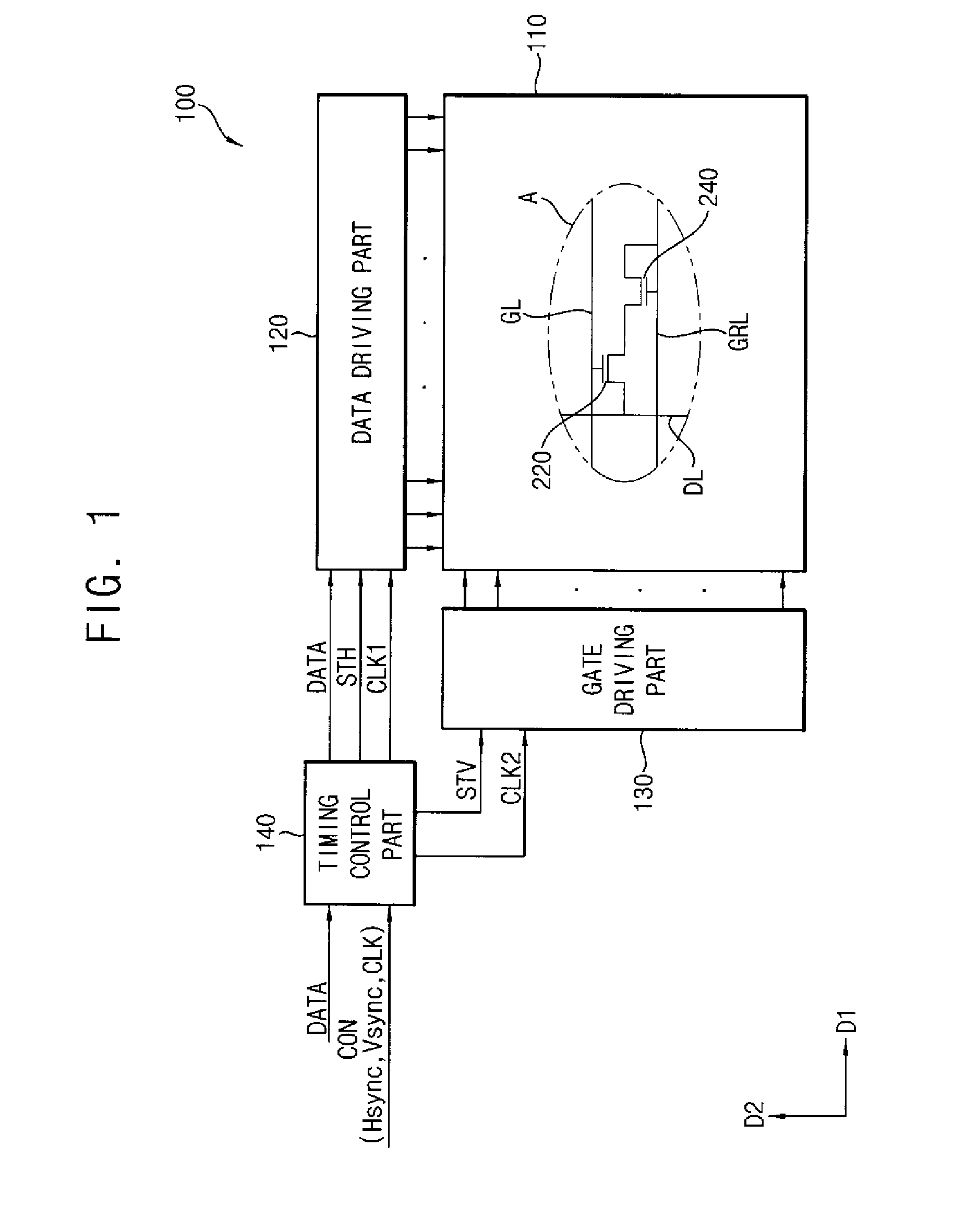
  • Figure 1
    Figure 1
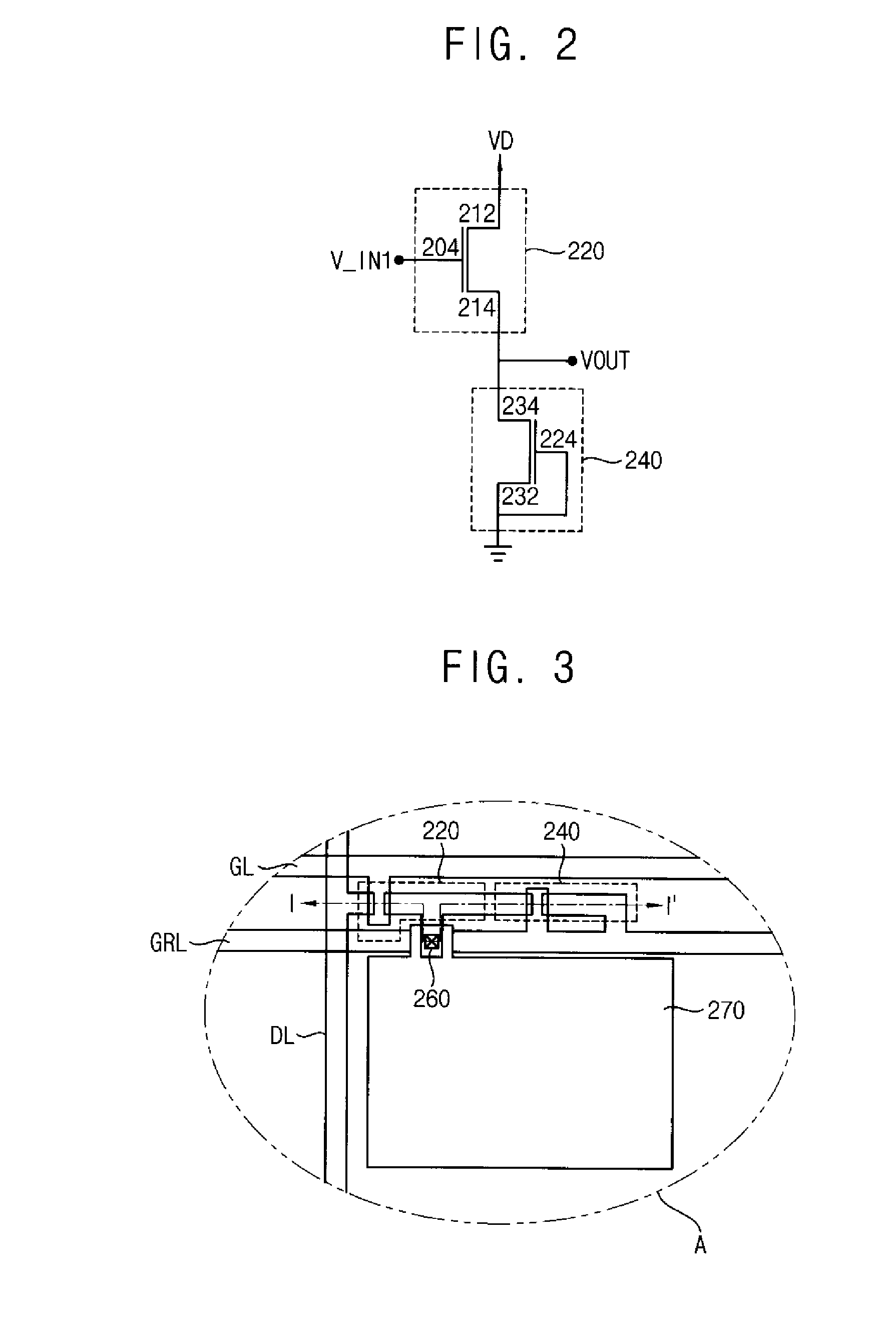
  • Figure 2
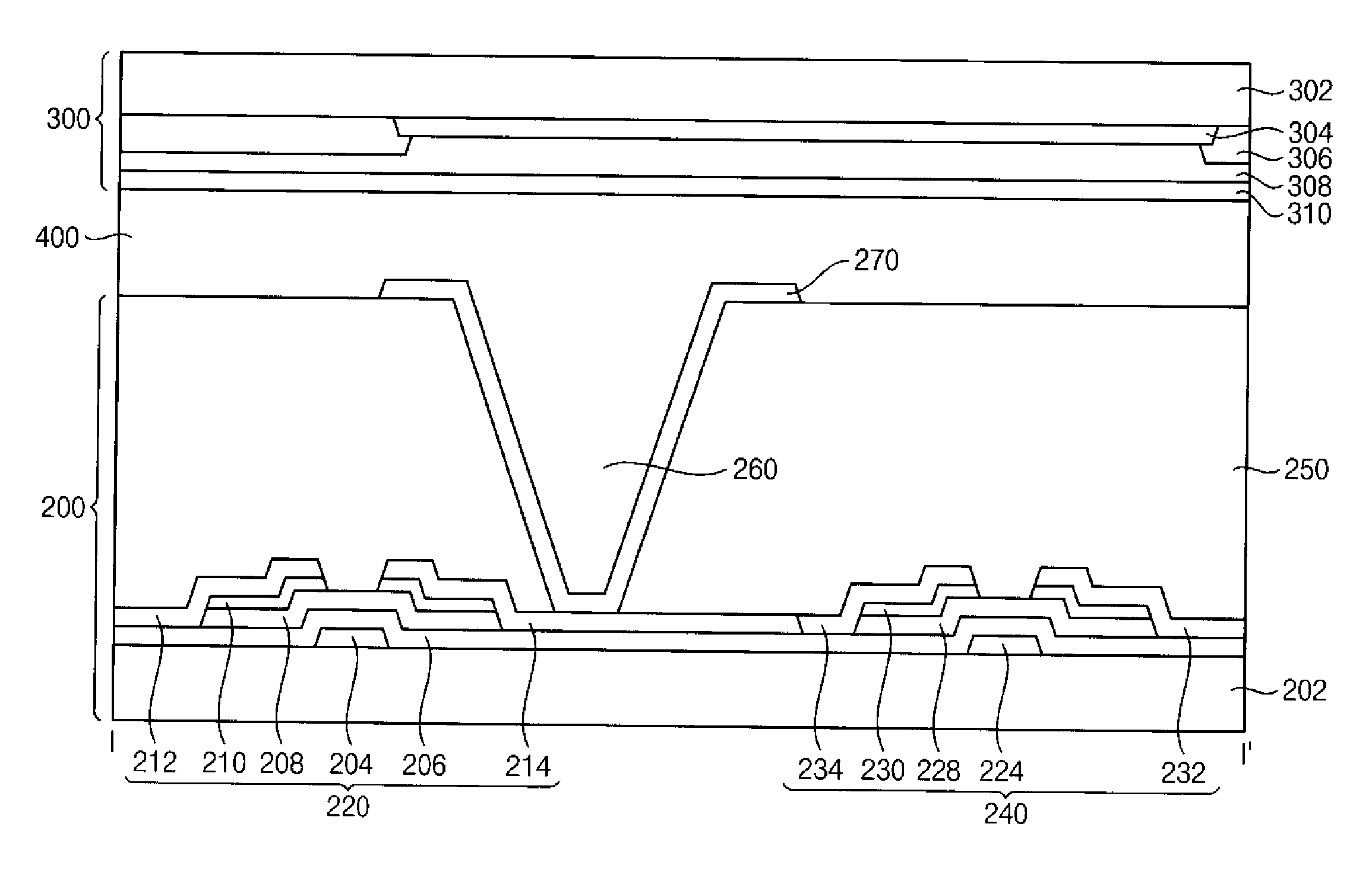
    Figure 2
  • Figure 3
    Figure 3
Patent Text Reader

Abstract

A display substrate includes a substrate, a switching element, a pixel electrode, and a light sensing part. The switching element is disposed on the substrate and is electrically connected to a gate line and a data line. The pixel electrode is electrically connected to the switching element. The light sensing part is electrically connected to the switching element and the pixel electrode, and is configured to control a grayscale of a pixel according to a brightness of an external light. The pixel includes the pixel electrode.
Need to check novelty before this filing date? Find Prior Art

Description

CROSS-REFERENCE TO RELATED APPLICATION

[0001] This application claims priority from and the benefit of Korean Patent Application No. 10-2012-0109772, filed on Oct. 4, 2012, which is hereby incorporated by reference for all purposes as if fully set forth herein.BACKGROUND

[0002] 1. Field

[0003] Exemplary embodiments of the present invention relate to a display substrate, a method of manufacturing the display substrate, and a display panel having the display substrate. More particularly, exemplary embodiments of the present invention relate to a display substrate used in a display apparatus, a method of manufacturing the display substrate, and a display panel having the display substrate.

[0004] 2. Discussion of the Background

[0005] A display apparatus, such as a liquid crystal display apparatus, an electrophoretic display apparatus, and a micro electro-mechanical system (MEMS) display apparatus, includes a display panel configured to display an image.

[0006] In a relatively bright environment, ...

Examples

Embodiment Construction

[0025]The invention is described more fully hereinafter with reference to the accompanying drawings, in which embodiments of the invention are shown. This invention may, however, be embodied in many different forms and should not be construed as limited to the embodiments set forth herein. Rather, these embodiments are provided so that this disclosure is thorough, and will fully convey the scope of the invention to those skilled in the art. In the drawings, the size and relative sizes of layers, regions, films, panels, etc., may be exaggerated for clarity. Like reference numerals denote like elements.

[0026]It will be understood that when an element such as a layer, film, region, or substrate is referred to as being “on” or “connected to” another element, it can be directly on or directly connected to the other element, or intervening elements may be present. In contrast, when an element is referred to as being “directly on” or “directly connected to” another element, there are no ot...