Display panel and pixel array thereof

Active Publication Date: 2015-10-29
AU OPTRONICS CORP
View PDF0 Cites 14 Cited by
  • Summary
  • Abstract
  • Description
  • Claims
  • Application Information

AI Technical Summary

Benefits of technology

[0096]In summary, the display panel of the present invention has the pixel array including a plurality of 2×6 sub-pixel matrixes. Each of the sub-pixel matrixes includes four brightness sub-pixel(s) (regions), four first sub-pixel(s) (regions), and four sub-pixel(s) (regions). All of the first sub-pixel(s) (regions) and the second sub-pixel(s) (regions) are disposed around the brightness sub-pixel(s) (regions), and the first sub-pixel(s) (regions) and the second sub-pixel(s) (regions) are respectively disposed at two adjacent sides of the corresponding brightness sub-pixel(s) (regions). Or, there are five brightness sub-pixel(s) (regions). All of the first sub-pixel(s) (regions) and the second sub-pixel(s) (regions) are disposed around the brightness sub-pixel(s) (regions), and the first sub-pixel(s) (regions) and the second sub-pixel(s) (regions) a

Problems solved by technology

A tolerance space is formed between any two immediately adjacent sub-pixels, such that the conventional AMOLED is hard to achieve high aperture ratio or high resolution.
Moreover, t

Method used


Image

  • Display panel and pixel array thereof
  • Display panel and pixel array thereof
  • Display panel and pixel array thereof

Examples


Example

[0055]Reference will now be made in detail to the present embodiments of the invention, examples of which are illustrated in the accompanying drawings. Wherever possible, the same reference numbers are used in the drawings and the description to refer to the same or like parts.

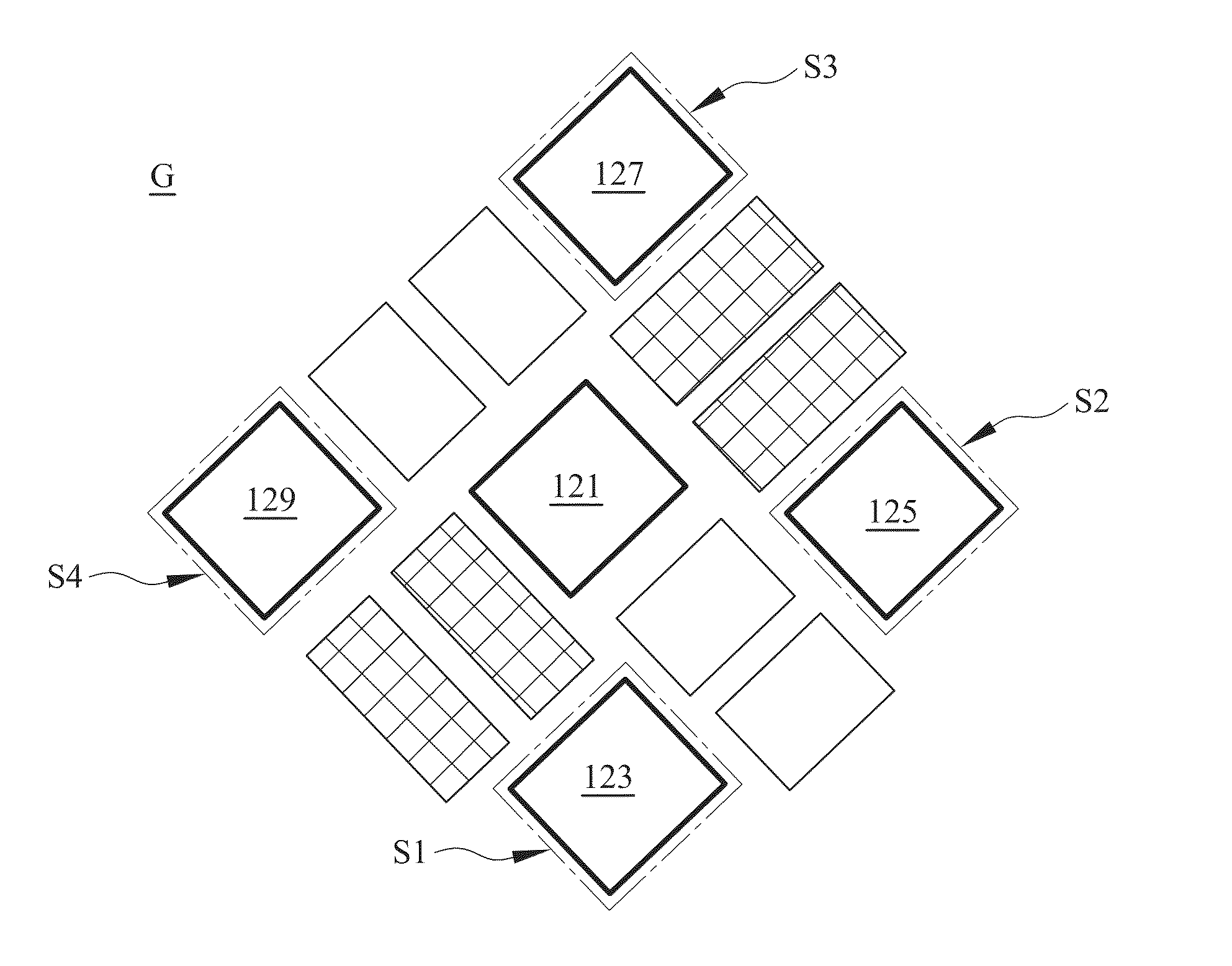
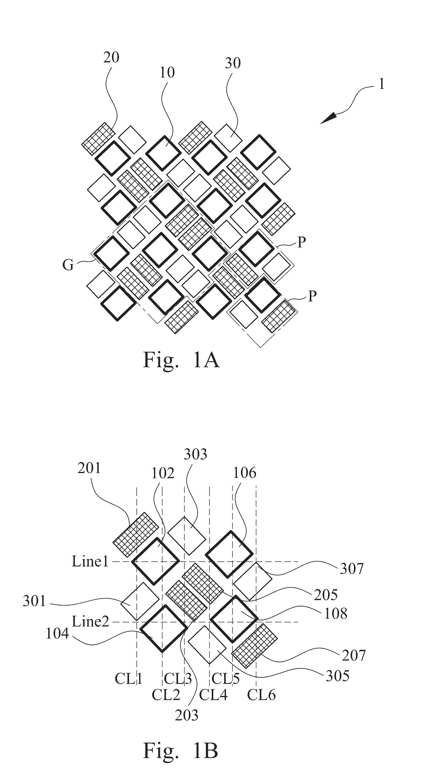
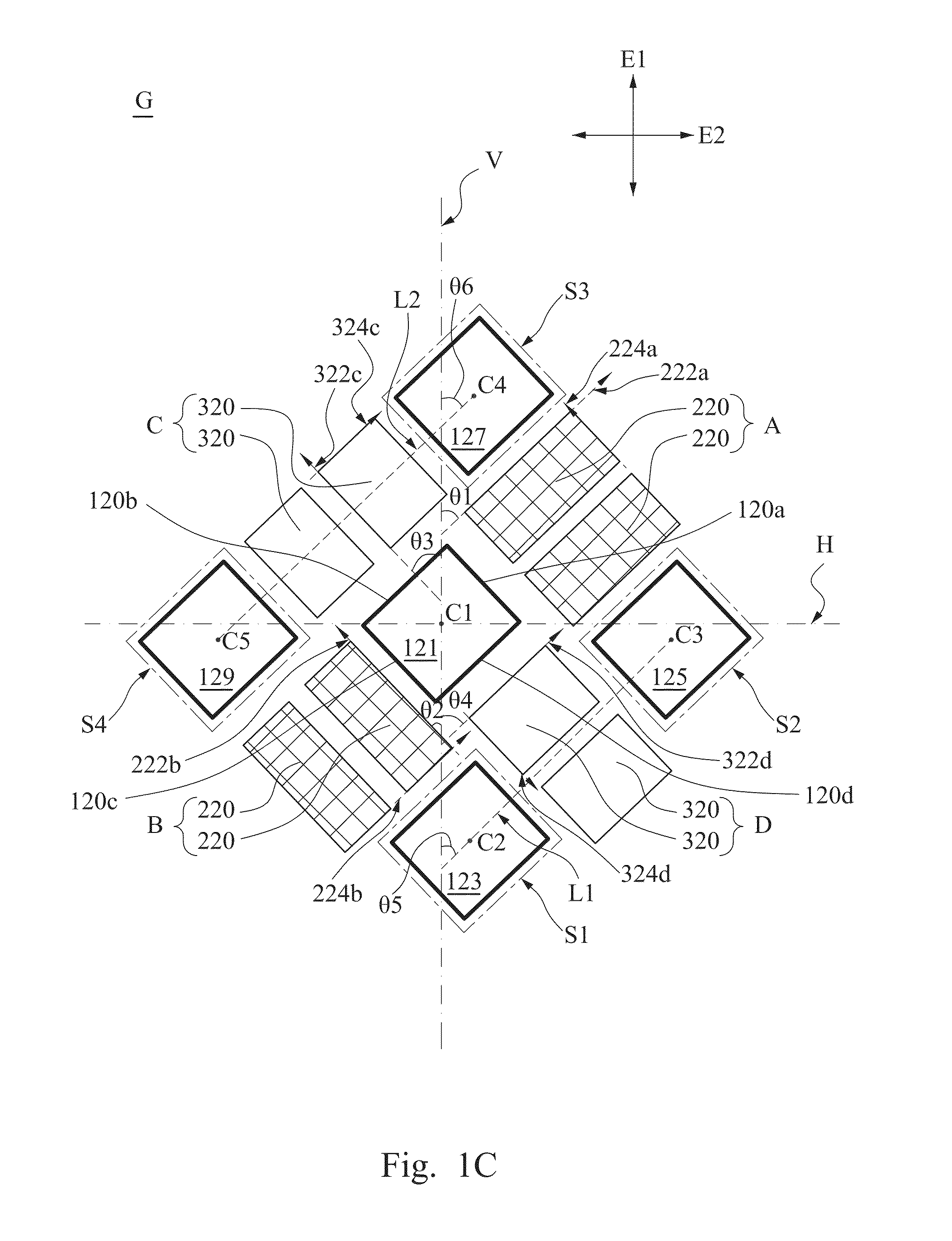
[0056]FIG. 1A is a schematic diagram of a pixel array 1 of a display panel according to one embodiment of the present disclosure, FIG. 1B is a schematic diagram of a single sub-pixel matrix of the pixel array 1 of FIG. 1A, and FIG. 1C is a schematic diagram of a single pixel group G of the pixel array 1 of FIG. 1A.

[0057]Reference is made to FIG. 1A. The display panel of this embodiment may be a display panel of an organic light emitting diode (OLED) display, having the pixel array 1. The pixel array 1 is composed by three different kinds of sub-pixels, that is, brightness sub-pixels (also called brightness sub-pixel regions) 10, blue sub-pixels (also called blue sub-pixel regions) 20, and red sub-pixels (also ...


PUM


Abstract

A pixel array includes a plurality of pixel groups, each of which includes a plurality of brightness sub-pixel regions, a plurality of first sub-pixel regions, and a plurality of second sub-pixel regions. Each brightness sub-pixel regions has a first side, a second side, a third side, and a fourth side. The first sub-pixel regions include a first group and a second group, and the second sub-pixel regions include a third group and a fourth group. The first, the second, the third, and the fourth groups are respectively disposed at the first, the third, the second, and the fourth sides of the first brightness sub-pixel region. Extension lines of long directions of the first, the second, the third, and the fourth groups respectively interlace a vertical baseline at a first angle θ1, a second angle θ2, a third angle θ3, and a fourth angle θ4. 0°<θ1<90°, 0°<θ2<90°, 0°<θ3<90°, and 0°<θ4<90°.

Description

RELATED APPLICATIONS[0001]This application claims priority to Chinese Application Serial Number 201410171459.8, filed Apr. 25, 2014, and Chinese Application Serial Number 201410358992.5, filed Jul. 25, 2014, which is herein incorporated by reference.BACKGROUND[0002]1. Field of Disclosure[0003]The present invention relates to a pixel array, especially relates to a pixel array of a display panel.[0004]2. Description of Related Art[0005]Recently, portable display panels have gradually replaced regular displays. Compared to other display panels, auto-luminescence displays such as organic or inorganic light-emitting displays have more superiorities of wide viewing angles, good contrast, and high response speeds. Therefore, the organic or inorganic light emitting displays, especially organic light emitting diode (OLED) displays composed by organic materials, have been widely focused as the next generation displays. Compared to the inorganic light emitting displays, the OLED displays have ...

Claims


Application Information

Patent Timeline
IPC IPC(8): H01L27/32
CPCH01L27/3218H01L27/3276H01L27/3216H01L27/3213H10K59/351H10K59/352H10K59/353H10K59/131
Inventor SHEN, SHIH-MINGLEE, MENG-TINGYANG, HSUEH-YEN
Owner AU OPTRONICS CORP
Why Eureka
Try Eureka