

Flexible display and manufacturing method therefor
A flexible display and manufacturing method technology, which is applied to electric solid-state devices, semiconductor devices, electrical components, etc., can solve problems such as defects, abnormal display, uneven surface, etc., so as to improve the problem of surface protrusions of the film layer and increase the process yield , the effect of good display quality
- Summary
- Abstract
- Description
- Claims
- Application Information
AI Technical Summary
Problems solved by technology
Method used
Image

Examples
experiment example 1
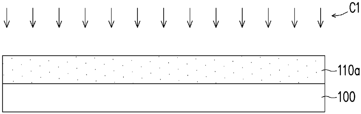
[0042] The following will introduce examples 1 to 6 and their comparisons using different first curing temperatures (hereinafter represented by T1) and second curing temperatures (hereinafter represented by T2) to respectively cure the first flexible layer and the second flexible layer. The flexible displays of Example 1 to Comparative Example 2. Moreover, the measurement of the number of air bubbles between the first flexible layer and the buffer layer was carried out 3 times in three process stages for the flexible displays of Examples 1 to 6 and Comparative Examples 1 to 2, wherein the three process stages They are: 1) after curing the first flexible layer and before forming the buffer layer; 2) after performing the heat treatment process on the amorphous silicon layer and before performing the excimer laser annealing process; 3) after performing the heat treatment process on the interlayer insulating material layer and before forming the second metal layer. The above-ment...
experiment example 2
[0052] Please refer to figure 2 , figure 2 Static thermomechanical analysis spectra of the second flexible layer of the flexible display of Examples 7 to 9 and Comparative Example 3 are shown. exist figure 2 The x coordinate in is the deformation of the second flexible layer (in ppm), the y coordinate is the ambient temperature (in °C), and the slope is the coefficient of thermal expansion (in ppm / °C). In addition, in figure 2 Among them, the second flexible layer respectively has a temperature lower than the first glass transition temperature ( figure 2 The first coefficient of thermal expansion at Tg1), between the first glass transition temperature and the second glass transition temperature ( figure 2 The second coefficient of thermal expansion when it is between Tg2 and the third coefficient of thermal expansion that is greater than the second glass transition temperature.
[0053] Table 4 shows the parameter information used to prepare the second flexible laye...
PUM
| Property | Measurement | Unit |
|---|---|---|
| Thickness | aaaaa | aaaaa |
| Thickness | aaaaa | aaaaa |
Abstract
Description
Claims
Application Information