Amplifier, circuit for trimming a bias voltage, method for amplifying an input signal and method for trimming a bias voltage

a technology for amplifying input signals and circuits, applied in amplifiers, dc-isolation amplifiers, semiconductor devices/discharge tubes, etc., can solve problems such as overall limited bias voltage, drift of bias voltage compared to a state, and energy may be conserved, so as to avoid distortion, optimal properties, and optimal power consumption

Active Publication Date: 2020-02-13
ADVANTEST CORP
View PDF0 Cites 0 Cited by
  • Summary
  • Abstract
  • Description
  • Claims
  • Application Information

AI Technical Summary

Benefits of technology

[0033]In embodiments, the circuit is configured to trim the bias voltage based on a cross current through the amplifying device. Trimming the bias voltage based on a cross current enables keeping the power consumption of the amplifying device at a moderate level and avoiding distortions based on an incorrectly adjusted cross current of the amplifying device. Thereby, a glitch in an amplified signal, e.g. the output signal of the amplifier, can be avoided, e.g., such that positive and negative half waves may be reproduced correctly in the output signal of the amplifier.
[0034]In embodiments, the circuit is configured to trim the bias voltage based on a measurement of the characteristic of an output signal of the amplifying device. Using a measurement of the characteristic of an output signal of the amplifying device enables adjusting the bias voltage such that the amplifying device may be operated in an operation point. The operation point may have optimal properties for a usage of the amplifying device. For example: to provide an appropriate amplification of an input signal and a specified cross current, e.g., such that an appropriate amplification can be achieved and such that a power consumption is optimal while avoiding distortions in an output signal of the amplifier.

Problems solved by technology

Moreover, considering the aging of components, characteristics of electric or electronic components may change, leading to a drift of the bias voltage compared to a state after manufacturing.
Moreover, when ensuring operation of the amplifying device at an operating point, energy may be conserved compared to an unadjusted operating point, e.g. causing a too large cross current to be flowing through a transistor.
Moreover, the regulator is configured to limit the bias voltage based on a voltage drop over the second resistor, to thereby limit a voltage drop over the first resistor, leading to an overall limited bias voltage.
Thus, limiting a maximum voltage at the second resistor leads to an overall voltage over the first and the second resistor, e.g., the bias voltage, which is also limited.
Thereby, the circuit provides a limited voltage drop over the first resistor and the second resistor, leading to an overall limited bias voltage.

Method used


Image

  • Amplifier, circuit for trimming a bias voltage, method for amplifying an input signal and method for trimming a bias voltage
  • Amplifier, circuit for trimming a bias voltage, method for amplifying an input signal and method for trimming a bias voltage
  • Amplifier, circuit for trimming a bias voltage, method for amplifying an input signal and method for trimming a bias voltage

Examples


Embodiment Construction

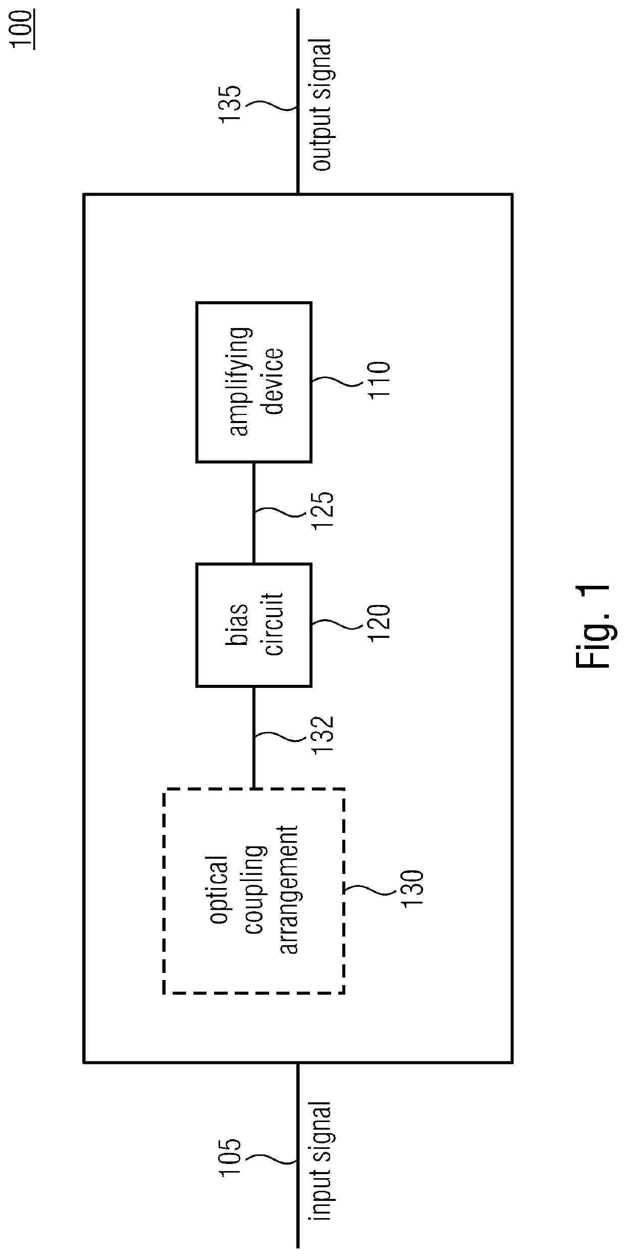
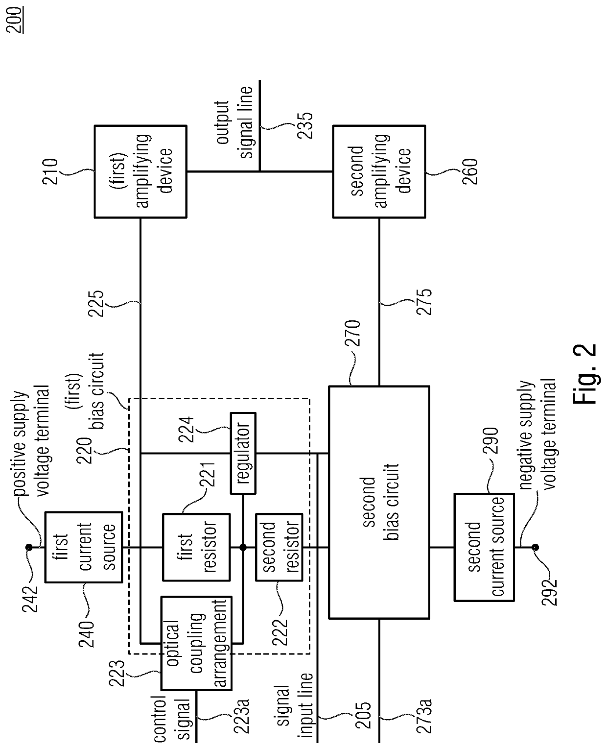
[0052]FIG. 1 shows a block diagram of an amplifier 100 according to embodiments of the invention. The amplifier 100 comprises an amplifying device 110, a bias circuit 120 and an optical coupling arrangement 130 (which may be a part of the bias circuit 120 or which may be an external component). Moreover, the amplifier 100 takes as input an input signal 105 and provides an amplified input signal as the output signal 135.

[0053]The bias circuit 120 is configured to provide a bias voltage for the amplifying device 110, wherein the bias circuit 120 is configured to provide the bias voltage 125 in dependence on an output signal 132 of the optical coupling arrangement 130 which provides for an electrical isolation. Further, the amplifying device 110 may be configured to work at an operation point. Therefore, a bias voltage 125 is provided to the amplifying device 110 by the bias circuit 120. As the bias voltage 125 may deviate from a desired voltage, e.g., which may be used for keeping the...


PUM


Abstract

An amplifier includes an amplifying device and a bias circuit for providing a bias voltage for the amplifying device. The bias circuit is configured to provide the bias voltage in dependence of an output signal of an optical coupling arrangement which provides for electrical isolation.

Description

CROSS-REFERENCES TO RELATED APPLICATION[0001]This application is a continuation of copending International Application No. PCT / EP2017 / 060254, filed Apr. 28, 2017, which is incorporated herein by reference in its entirety.[0002]Embodiments of the present invention relate to providing a bias voltage to an amplifying device.BACKGROUND OF THE INVENTION[0003]It has been found that power amplifiers involve a thorough control of the output stage to optimize signal fidelity versus a standby current consumption. It has been found that to ensure performance a cross current in output transistors may need to be adjusted well. It has been recognized that this adjustment involves exact process control or trimming (potentiometer) before the shipping of amplifier products. Some traditional designs use high voltage current mirrors to transfer a ground-related trim signal to a level of a power output stage.[0004]In US 2014 / 0300413 A1 a power transistor gate driver is disclosed.[0005]In US 2011 / 015681...

Claims


Application Information

Patent Timeline
Patent Type & Authority Applications(United States)
IPC IPC(8): H03F1/02H03F1/30H03F3/21
CPCH03F1/0205H03F1/301H03F2200/18H03F2200/21H03F3/211H03F2200/276H03F2200/393H03F1/0261H03F1/308H03F3/085H03F3/21H03F3/3022H03F2203/30003H03F2203/30066
Inventor THOMA, ANTON
Owner ADVANTEST CORP
Why Eureka
Try Eureka