
Method and apparatus for measuring dopant profile of a semiconductor
a technology of semiconductor and dopant profile, which is applied in the direction of semiconductor/solid-state device testing/measurement, instrumentation, individual semiconductor device testing, etc., can solve the problems that all prior art techniques generally do not have a very high sensitivity and/or spatial resolution to meet the demands of integrated circuit manufacturing at submicron levels, and the sensitivity of some prior art techniques tends to decreas
- Summary
- Abstract
- Description
- Claims
- Application Information
AI Technical Summary
Problems solved by technology
Method used
Image

Examples
Embodiment Construction
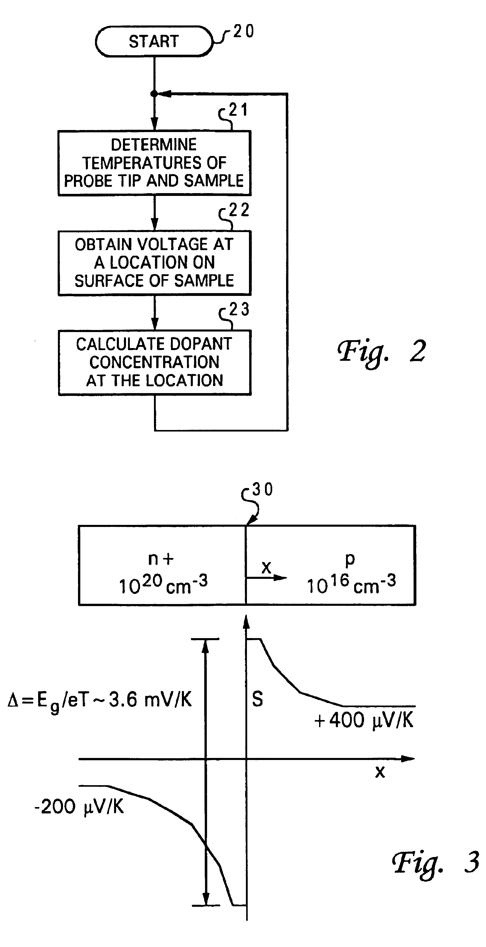
[0013]The Seebeck coefficient of a semiconductor depends on the concentration of dopants within the semiconductor. For example, the Seebeck coefficient S of an n-type silicon is S=1-e T(EC-EF+2kBT)≈-kBeln nNc
where[0014]e=charge[0015]T=temperature[0016]n=dopant concentration[0017]EC=conduction band energy[0018]EF=Fermi energy[0019]kB=Boltzman constant[0020]Nc=constant
Thus, the dopant concentration of a semiconductor can be determined by measuring the Seebeck coefficient of the semiconductor via n=Ncexp[-eSkB]
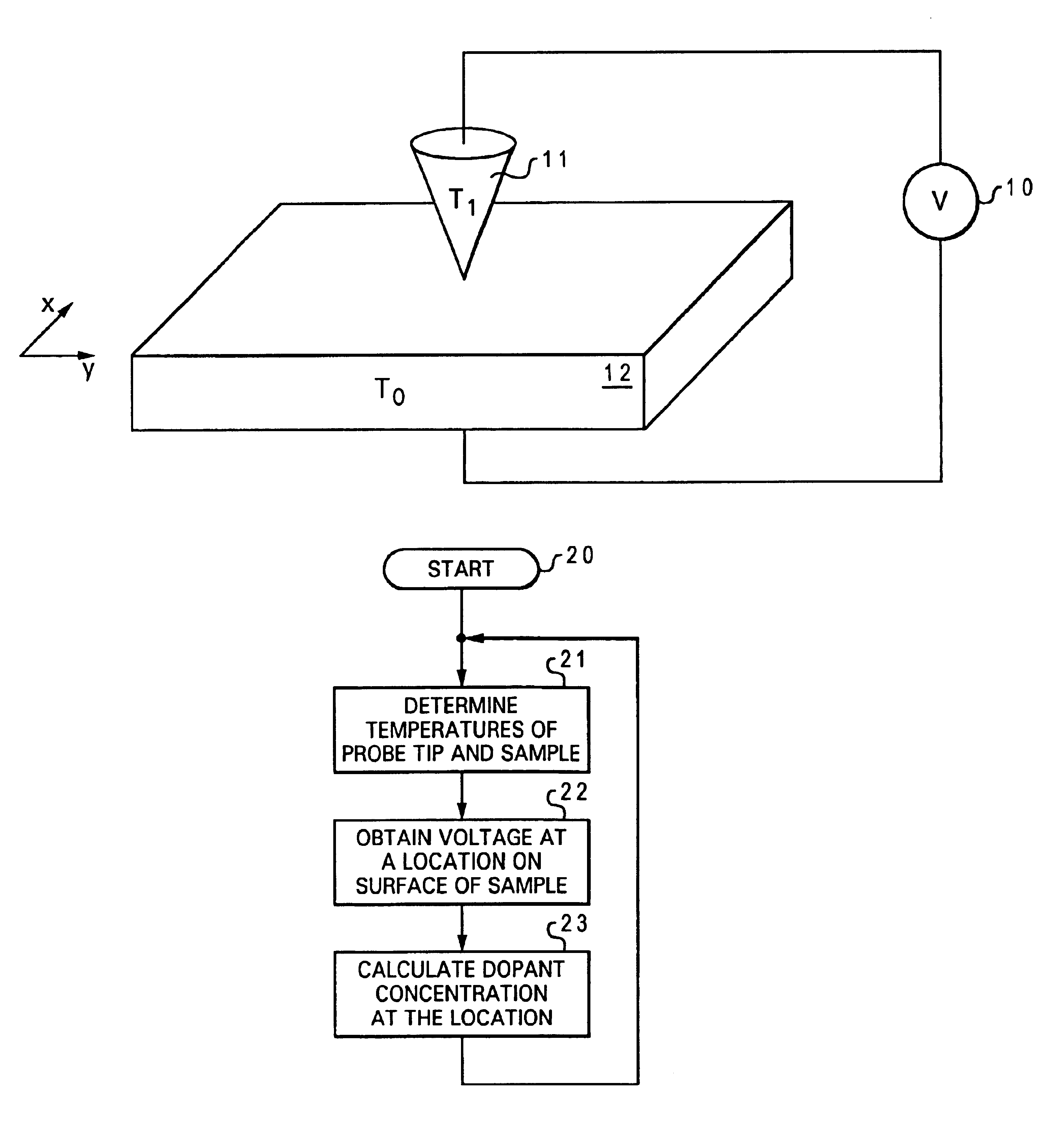
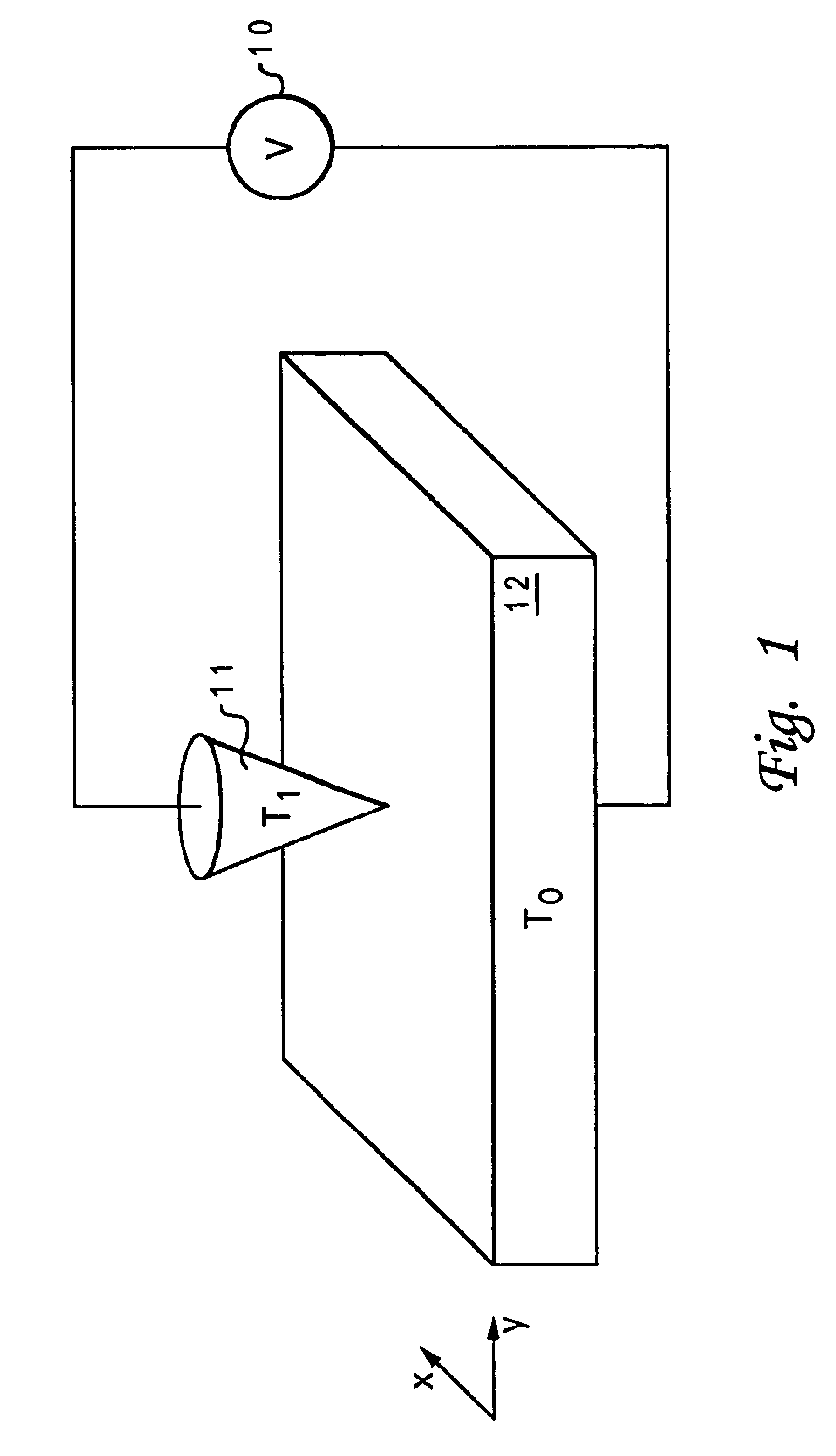
The Seebeck coefficient can be measured by using Scanning Thermoelectric Microscopy (STEM), as detailed in Ghoshal, Miner and Majumdar, Proc. 19th, Int. Thermoelectrics Conference, p. 221 (2000), the pertinent of which is incorporated herein by reference, or Scanning Chemical Potential Microscopy (SCPM), as detailed in Williams and Wickramasinghe, Nature, 344, p. 317 (1990), the pertinent of which is incorporated herein by reference.
[0021]Referring now to the drawings...
PUM
| Property | Measurement | Unit |
|---|---|---|
| channel length | aaaaa | aaaaa |
| concentration | aaaaa | aaaaa |
| voltage | aaaaa | aaaaa |
Abstract
Description
Claims
Application Information