Aligned logic cell grid and interconnect routing architecture

a logic cell and grid technology, applied in the field of integrated circuits, can solve problems such as inefficient use, mismatch or sub-optimal layout, and inefficient layout between

Active Publication Date: 2007-10-23
ICERA INC
View PDF7 Cites 4 Cited by
  • Summary
  • Abstract
  • Description
  • Claims
  • Application Information

AI Technical Summary

Problems solved by technology

In the design of conventional cell library architecture, a mismatch or sub-optimal layout may exist between transistor pitch and routing pitch.
The sub-optimal layout of conventional transistor / routing pitch may result in inefficient use of IC area impacting IC performance therefore, it is desirable to remove the inefficient layout between transistor and routing pitches.
An associated problem occurs with the routing efficiency when a metal width or spacing greater than the minimum is required which is discussed with reference to FIG. 3.
This approach is clearly inefficient when a small increase, for example 1.5×, in spacing is required.
Similarly, this is inefficient if small increases, for example 1.5×, in width is required.
Although with this configuration, a maximum increase of 3× minimum spacing, or 5× minimum width with 3×3 via arrays, is achievable, these limits are excessive and routing efficiency and cell packing density is jeopardised.
Often attempts to reduce the cross-talk by increasing spacing to 1.5×-2× or to avoid electromigration by increasing width to 3× or increasing the number of vias to 2×2, have resulted in a conventional architecture that is inefficient and wasteful with respect to IC area and cell packing density.

Method used


Image

  • Aligned logic cell grid and interconnect routing architecture
  • Aligned logic cell grid and interconnect routing architecture
  • Aligned logic cell grid and interconnect routing architecture

Examples


Embodiment Construction

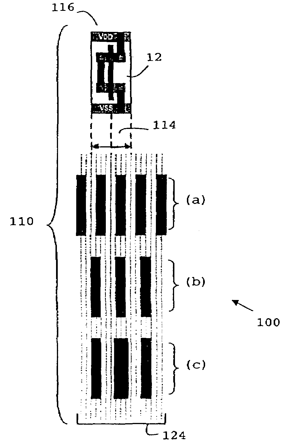
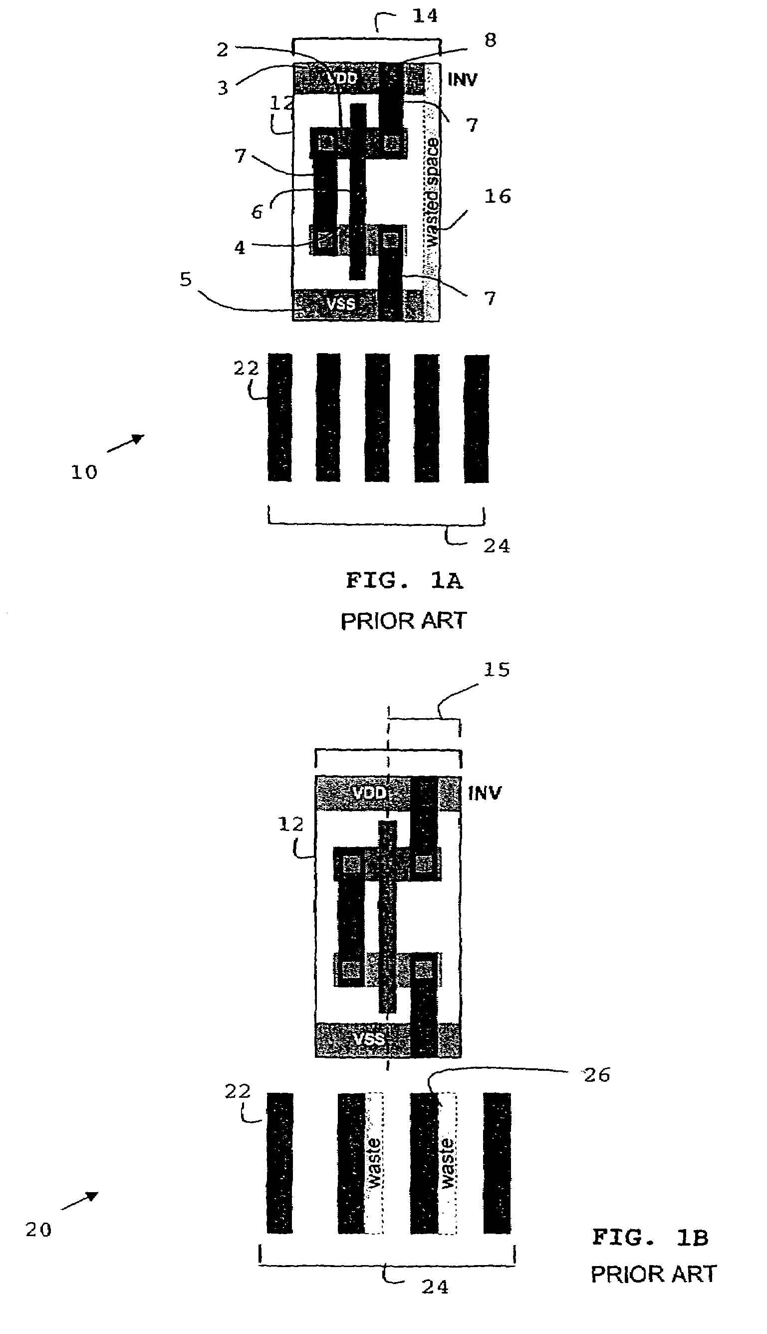
[0023]FIG. 4 is a grid 100 for a logic cell 12 having a cell pitch 110 aligned with a reduced grid routing pitch 124 in accordance with an embodiment of the invention. The routing pitch is defined by a highest common denominator of the transistor pitch 114 and the routing pitch 24 as discussed with FIG. 1A. It will be appreciated that the highest common denominator is an example and is not necessarily the factor chosen to define the routing pitch, as discussed in more detail below. For the purpose of illustrating this embodiment of the invention, references and comparisons are made to FIG. 1A.

[0024]In an embodiment, the reduced routing pitch 124 is equivalent to 1 / q of the initial routing pitch 24 where q is an integer. In this embodiment ¼ is shown. It will be appreciated that other reduced routing pitches may be chosen, for example ⅕, ⅙, or the like. Similarly, increased routing pitches ½ or ⅓ may be chosen, however, the granularity may not be sufficiently small The reduced routin...


PUM


Abstract

A method for defining an aligned logic cell grid and interconnect layout of a semiconductor integrated circuit having a logic cell is disclosed. The interconnect layout is resized in accordance with a highest common denominator of an initial routing pitch of the interconnect layout and a transistor pitch of the logic cell. The cell grid is aligned with the resized routing pitch which provides efficient routing density and transistor performance, minimizes excess transistor area and wire routing waste while maximizing cell packing density.

Description

FIELD OF THE INVENTION[0001]This invention relates to integrated circuits, and more particularly to the interconnect layout of transistor pitch and wire routing pitch within a standard cell library architecture for large scale integration of semiconductor integrated circuits.BACKGROUND[0002]Conventional standard cell library architecture of semiconductor integrated circuits (IC) primarily contain a logic cell layout based in a metal oxide semiconductor environment, in particular a complimentary metal oxide semiconductor (CMOS) environment. Cell library designers strive to maximise the packing density of the logic cells within the standard cell library. Logic cells are composed of transistors that are arranged into base patterns or gate arrays of different types of logical operations, and then fabricated into an application specific IC (ASIC) to perform a specific function. A conventional ASIC layout is typically defined by an array of logic cells arranged in adjacent rows. Such an a...

Claims


Application Information

Patent Timeline
Patent Type & Authority Patents(United States)
IPC IPC(8): G06F17/50
CPCG06F17/5068G06F30/39
Inventor MORTON, SHANNON VANCE
Owner ICERA INC
Why Eureka
Try Eureka