Current source circuit, display device using the same and driving method thereof

a current source circuit and display device technology, applied in static indicating devices, instruments, electroluminescent light sources, etc., can solve the problems of difficult to perform accurate setting operations, fluctuation of current flowing to light emitting elements, and high time consumption of accurate setting operations, so as to improve accuracy, reduce the influence of transistor variation, and improve the speed of setting operations

Inactive Publication Date: 2008-01-15
SEMICON ENERGY LAB CO LTD
View PDF22 Cites 33 Cited by
  • Summary
  • Abstract
  • Description
  • Claims
  • Application Information

AI Technical Summary

Benefits of technology

[0017]It is an object of the present invention to provide a display device that can reduce influence on variation in transistors of pixels. Further, another object of the present invention is to provide a display device in which a light emitting element is to emit light with constant luminance, irrespective of changes in current characteristic caused by deterioration or the like.
[0020]In this way, by switching the connection states, the current value to be fed to the current source circuit can be increased. As a result, a setting operation can be performed more precisely in a shorter period of time.
[0026]According to the present invention, a light emitting element can emit light at constant luminance irrespective of the changes in current characteristic due to deterioration, for example. Furthermore, according to the present invention, the current value for setting a current source circuit can be larger than driving current for causing a light emitting element to emit light. Therefore, the speed of the setting operation can be improved.
[0027]Since the current source circuit can output a constant amount of current, the influence of variation in transistors can be reduced. Video signals are different from current for setting the current source circuit. Therefore, video signals and current can be controlled independently. In other words, the current source circuit only feeds a constant amount of current, and video signals do not change the current value. Therefore, a setting operation can be performed at an arbitrary time and at arbitrary intervals.
[0028]As described above, according to the present invention, a display device can be provided which can express accurate gray scale and which can reduce uneven displays.

Problems solved by technology

However, an accurate setting operation needs much time, unless the current value of the signal current (video signal) is set to high value, because a parasitic capacitance (e.g., a capacitance at intersection of wirings) or resistance of wirings are generated in signal lines or the like provided in a pixel portion of a display device.
Therefore, it is difficult to perform an accurate setting operation.
This causes a fluctuation of current flowing to a light emitting element and a display unevenness.
It is difficult to perform an accurate setting operation when the signal current supplied to a pixel is small, that is, luminance is small.
On that account, there is such a high risk that it is impossible to cause the pixel to emit light with accurate luminance.
However, a relationship between a flowing current and a voltage applied to a light emitting element is changed due to a temperature in surrounding environment or deterioration of a light emitting element.
As a result, burning-in in a display or the like occurs.

Method used


Image

  • Current source circuit, display device using the same and driving method thereof
  • Current source circuit, display device using the same and driving method thereof
  • Current source circuit, display device using the same and driving method thereof

Examples


embodiment mode 1

[0059]A specific structure of a current source circuit according to Embodiment Mode 1 will be described.

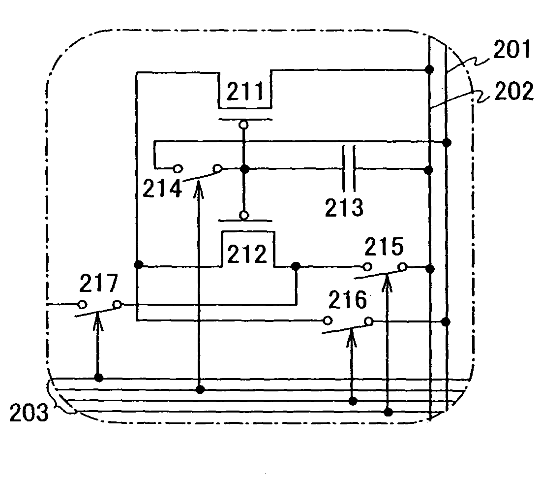
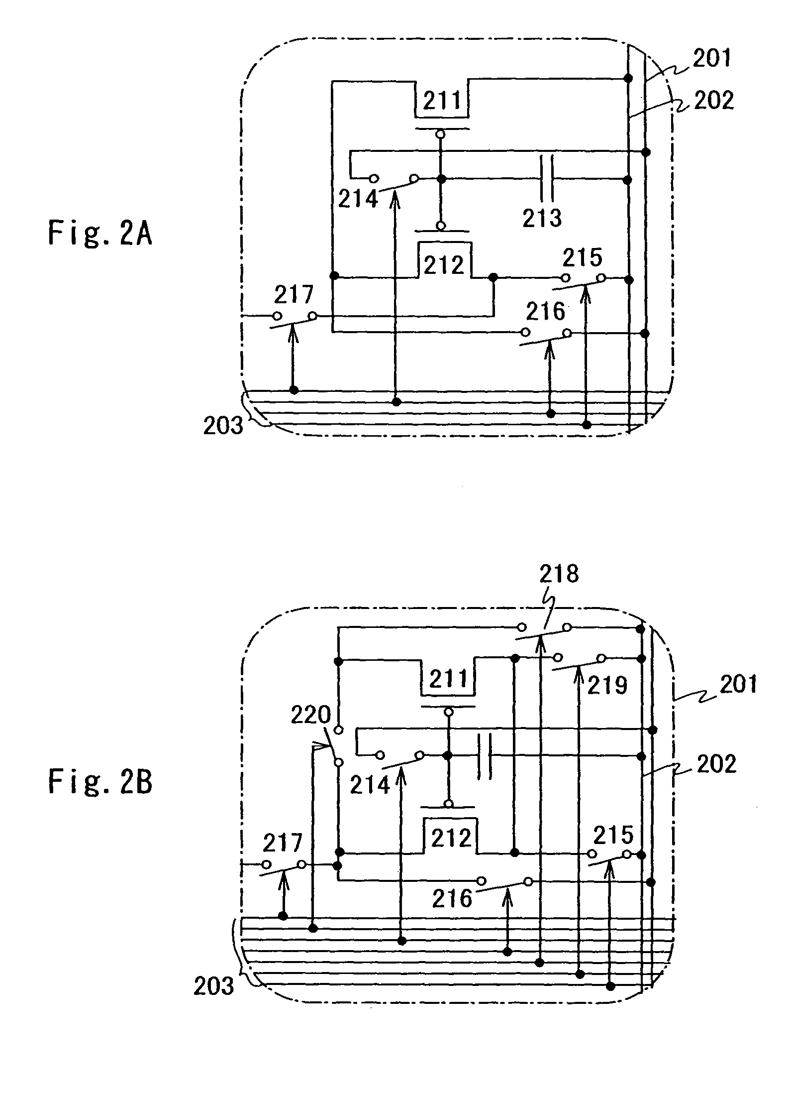
[0060]FIGS. 22A to 22C show a circuit structure where a driving element of the current source circuit has two transistors.

[0061]The current source circuit shown in FIGS. 22A to 22C has a first transistor 21, a second transistor 22, a capacitor element 23, a light emitting element 24, a current source line 25 and a power source line 26. The first transistor and second transistor have large gate capacitance and do not need capacitor elements when a leak current from each of the transistor falls in a permissible range. According to this embodiment mode, the first transistor and the second transistor are current source transistors, and the polarity is p-channel type.

[0062]FIG. 22A shows a current source circuit and a path that current flows during a setting operation. Each of FIGS. 22B and 22C shows a current source circuit and a path that current flows through during light emission. ...

embodiment mode 2

[0118]A specific pixel structure having a current source circuit for feeding current as shown in FIG. 22B during light emission according to a second embodiment will be described with reference to FIGS. 8A to 8C and FIG. 24.

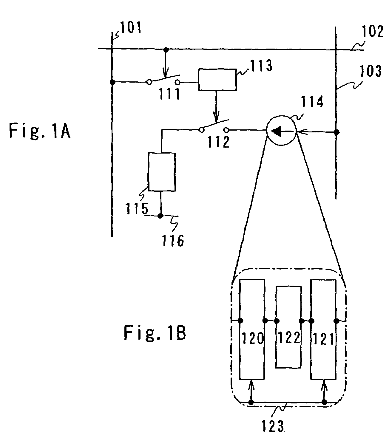
[0119]FIG. 8A shows an example of a pixel including the current source circuit shown in FIGS. 22A to 22C. The pixel includes a signal line 801, a first scanning line 802, a second scanning line 803, a third scanning line 804, a current source line 805, a power source line 806, a first transistor 811 for selection, a second transistor 812 for erasing, a third transistor 813 for driving, a fourth transistor 814 for light emission, a fifth transistor 815 and sixth transistor 816 for current source, which are current source transistors, a seventh transistor 817 for holding, an eighth transistor 818 for current input, a ninth transistor 819 for switching, a first storage capacitor 820, a second storage capacitor 821 and a light emitting element 822.

[0120]According to ...

embodiment mode 3

[0133]In this embodiment mode, a specific example of a pixel provided with current source circuit in which current flows in emitting light as shown in FIG. 22C is given with reference to FIGS. 9, 10, 11A, 11B, 12, 13, and FIGS. 25 to 27. FIGS. 22B and 22C are different in that the direction of current flow and the connections are different. However, both of them are essentially the same.

[0134]A pixel shown in FIG. 9 is an example for a pixel provided with a current source circuit in FIG. 22A to 22C. The second electrode of the fifth transistor 815 is connected to the second electrode of the sixth transistor 816. A tenth transistor 910 to a twelfth transistor 912 are provided and controlled by the third scanning line 804 in the pixel of FIG. 9.

[0135]The tenth transistor 910 is connected between the first electrode of the fifth transistor 815 that constitutes a current source transistor and the power source line 806. The eleventh transistor 911 is connected between the second electrod...


PUM


Abstract

In a display device having a light emitting element, an accurate setting operation needs much time, unless a current value of the signal current (video signal) is set to high value. On the contrary, the driving current value for causing a light emitting element to emit light is very small. Therefore, it is difficult to perform an accurate setting operation. However, according to the present invention, the current source circuit includes plural transistors. The plural transistors are connected in parallel when the setting operation is performed on the current source circuit, whereas the plural transistors are connected in series when the light emitting element is caused to emit light. Further, the speed of the setting operation is increased because a light emitting element is capable of emitting light with a constant luminance and a current value to set up a current source circuit is higher than a driving current value when a light emitting element emits light.

Description

BACKGROUND OF THE INVENTION[0001]1. Field of the Invention[0002]The present invention relates to an active matrix type display device and driving method thereof in which a transistor and a light emitting element are provided in each pixel and a current source circuit can control light emission of a pixel by each transistor. More particularly, the present invention relates to an active matrix type EL display device using an electroluminescence element as a light emitting element.[0003]2. Description of the Related Art[0004]An active matrix EL display device having a transistor which control a light emitting element and light emission of the light emitting element has been gathering attention in recent years. Such display device has advantages of superiority in response, operation with a low voltage, a wide view angle and the like. Therefore, the active matrix display device has attracted attention as a next generation flat panel display.[0005]Driving methods in the case where a multi...

Claims


Application Information

Patent Timeline
Patent Type & Authority Patents(United States)
IPC IPC(8): G09G3/30G09G3/20G09G3/32H01L51/50G09G3/36H05B33/14
CPCG09G3/325G09G3/2022G09G2300/0814G09G2330/02G09G2310/0251G09G2310/0262G09G2320/043G09G2300/0861G09G3/30
Inventor KIMURA, HAJIMEINUKAI, KAZUTAKA
Owner SEMICON ENERGY LAB CO LTD
Why Eureka
Try Eureka