Organic EL display device, electronic equipment, and method for manufacturing the same

a display device and organic technology, applied in the direction of discharge tube luminescnet screens, discharge tube/lamp details, electric discharge lamps, etc., can solve the problems of certain limits of the total thickness of the display panel, increase the number of manufacturing steps, and complicated manufacturing processes

Active Publication Date: 2008-03-11
ELEMENT CAPITAL COMMERCIAL CO PTE LTD
View PDF23 Cites 45 Cited by
  • Summary
  • Abstract
  • Description
  • Claims
  • Application Information

AI Technical Summary

Benefits of technology

[0006]However, when the organic EL display device is transferred to the final substrate by repeating the peeling transfer between substrates as many as two times, as described above, the number of manufacturing steps is increased, and the manufacturing process becomes complicated.

Problems solved by technology

However, when the organic EL display device is transferred to the final substrate by repeating the peeling transfer between substrates as many as two times, as described above, the number of manufacturing steps is increased, and the manufacturing process becomes complicated.
Consequently, even when a thin plastic substrate is used, there is a certain limit to reduction in the total thickness of the display panel.
Furthermore, the light radiated from an organic EL light emitting element located between the two substrates is emitted to the outside through one of the substrate and, thereby, a transmission loss is produced during passage through the substrate.

Method used


Image

  • Organic EL display device, electronic equipment, and method for manufacturing the same
  • Organic EL display device, electronic equipment, and method for manufacturing the same
  • Organic EL display device, electronic equipment, and method for manufacturing the same

Examples


Embodiment Construction

[0032]The exemplary embodiments of the present invention will be described bellow with reference to the drawings.

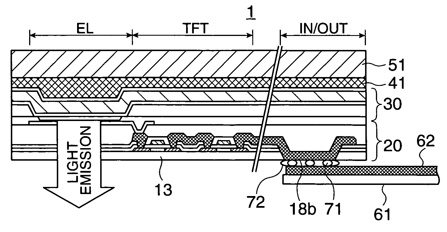
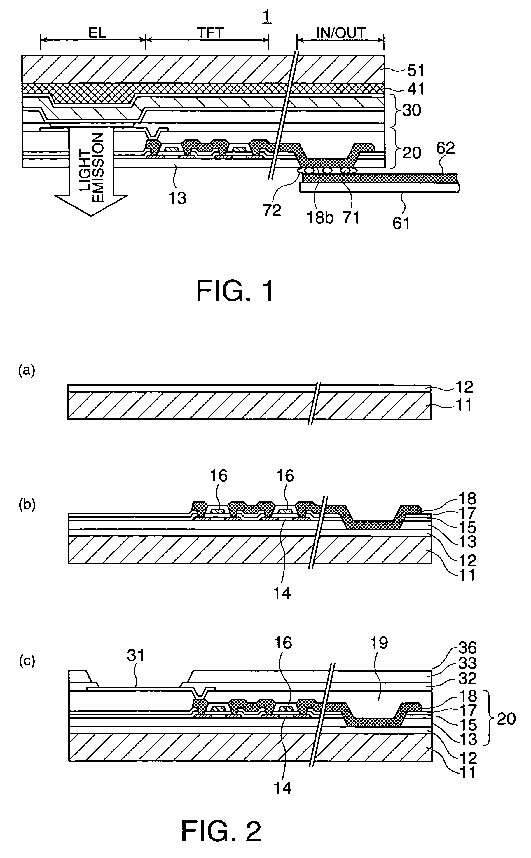
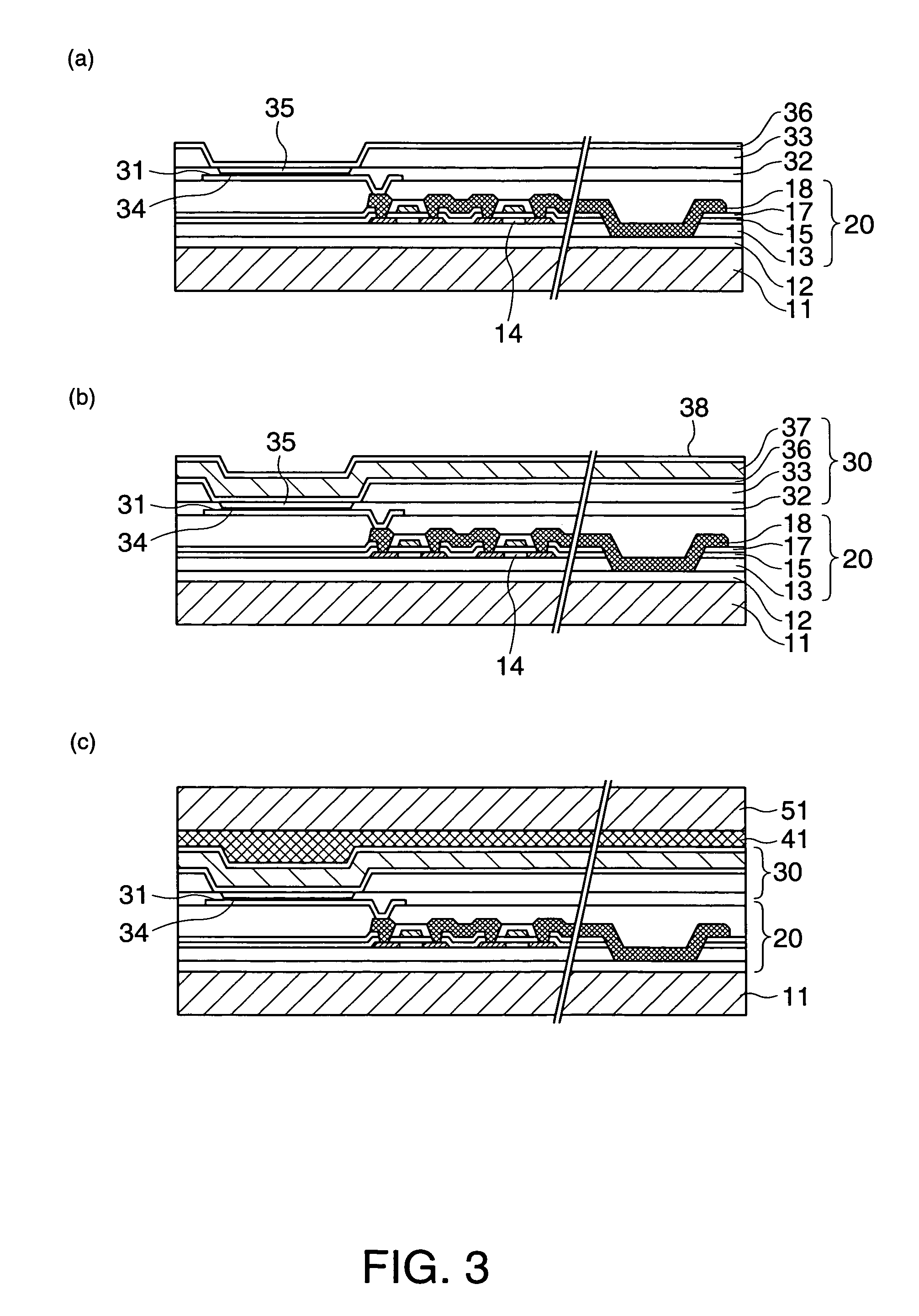
[0033]An organic EL display device according to an exemplary embodiment has a configuration in which a substrate provided to support a laminate including a TFT circuit layer, an organic EL light emitting layer, and the like doubles as a sealing substrate. Thereby, one of two substrates of an element-forming substrate and a sealing substrate is unnecessary. Consequently, the laminate is formed in order that a connection electrode is exposed at the back side. The resulting laminate is transferred to a final substrate through one transfer described below. The final substrate is used as a support substrate for the laminate and the sealing substrate. The light emitted from the organic EL light emitting layer is output toward the back side of the laminate while a glass substrate and the like do not intervene. The external circuit is connected to the back side of the laminate th...


PUM


Abstract

To provide a sheet-shaped organic EL display device having a reduced thickness, an organic EL display device includes a substrate serving as both a protective layer to reduce or prevent permeation of moisture, oxygen, and the like into the inside and a support layer for film formation, a laminate which is provided on a under layer by film formation and which includes a thin film circuit layer carrying an electric circuit and an organic EL light emitting layer carrying an organic EL light emitting element, and an adhesive layer joining the above-described laminate and the above-described substrate. The above-described organic EL light emitting element radiates the emitted light toward the above-described under layer side. In this manner, a low-profile organic EL display device can be provided.

Description

BACKGROUND OF THE INVENTION[0001]1. Field of Invention[0002]The present invention relates to an enhancement of an organic EL display device. In particular, it relates to an organic EL display device which can be prepared with a reduced thickness, electronic equipment including the same, and a method to manufacture the same.[0003]2. Description of Related Art[0004]With respect to related art semiconductor devices and the like, high-temperature treatment is included in the process of manufacturing laminates composed of required microstructures, thin film circuits, and the like on substrates. Therefore selection of elements constituting substrates and laminates may be restricted. For example, resin films, plastic substrates, and the like are not suitable for a high-temperature treatment.[0005]Consequently, for example, as described in Japanese Unexamined Patent Application Publication No. 2002-217391, a thin film circuit is formed on a heat-resistant element-forming substrate with a fi...

Claims


Application Information

Patent Timeline
Patent Type & Authority Patents(United States)
IPC IPC(8): H05B33/00H05B33/04H01L21/77H01L21/84H01L27/32H01L51/50H01L51/52H01L51/56H05B33/06H05B33/10
CPCH01L27/1214H01L27/1266H01L51/56H01L27/3244H01L27/3276H01L51/5237H10K59/12H10K59/131H10K50/844H10K71/00H05B33/10
Inventor UTSUNOMIYA, SUMIOKAMAKURA, TOMOYUKI
Owner ELEMENT CAPITAL COMMERCIAL CO PTE LTD
Why Eureka
Try Eureka