Pixel circuit and organic light emitting display using the same
a technology of light-emitting display and pixel circuit, which is applied in the direction of electroluminescent light sources, static indicating devices, instruments, etc., can solve the problem of limiting the uniformity of the tft array that can be fabricated by laser annealing process
- Summary
- Abstract
- Description
- Claims
- Application Information
AI Technical Summary
Benefits of technology
Problems solved by technology
Method used
Image


Examples
first embodiment
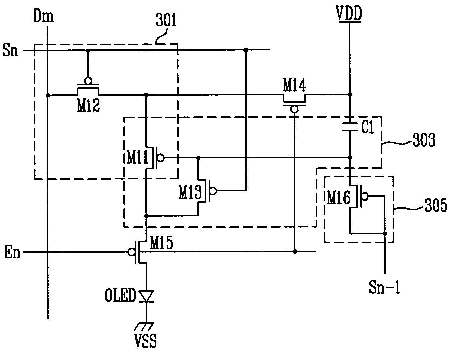
[0028]FIG. 2 is a circuit diagram of a pixel circuit in an organic light emitting display according to the present invention.
[0029]Referring to FIG. 2, the pixel circuit includes first through fifth transistors M11, M12, M13, M14, M15 and one capacitor C1. The first transistor M11 is used as a driving transistor to apply current to an organic light emitting diode (OLED) having a cathode connected to a second power line. The other second through fifth transistors M12, M13, M14 and M15 are used as a switching transistor. The first through fifth transistors M11 through M15 are each of a p-type transistor (or a transistor of a p-channel type). The OLED includes an multi-layered organic thin film containing a fluorescent or phosphoric organic compound, and an anode and a cathode connected to opposite terminals of the organic thin film.
[0030]In more detail, the first transistor M11 includes a source connected to a drain of the second transistor M12, a drain connected to a source of the fi...
second embodiment
[0046]According to the present invention, the fourth and fifth transistors can each be realized by an n-type transistor as well as the p-type transistor shown in FIG. 3. In the case of n-type fourth and fifth transistors, the n-type fourth and fifth transistors are operated by a reversed emission control signal as compared with the emission control signal for the p-type fourth and fifth transistors M14 and M15 shown in FIG. 3.
[0047]Thus, in a pixel circuit according to the second embodiment of the present invention, a voltage stored in a capacitor (e.g., the capacitor C1) is discharged through a transistor (e.g., the transistor M16) connected to the capacitor as a diode, and therefore the capacitor is initialized before the image data is programmed in the capacitor. As such, the discharging of voltage previously stored in (or the initializing of) the capacitor allows a later voltage corresponding to the data signal of the following frame to be securely stored in the capacitor. Furth...
PUM
 Abstract
Description
Claims
Application Information