Check patentability & draft patents in minutes with Patsnap Eureka AI!

Printed circuit board assembly

a printed circuit board and assembly technology, applied in the direction of printed circuit aspects, circuit thermal arrangements, electrical devices, etc., can solve the problems of high spatial integration, serious heat dissipation of printed circuit boards, and high power consumption of 30 kw or more, and achieve satisfactory thermal interface and wide conductive channels.

Active Publication Date: 2012-10-02
THALES HLDG UK
View PDF14 Cites 8 Cited by
  • Summary
  • Abstract
  • Description
  • Claims
  • Application Information

AI Technical Summary

Benefits of technology

The solution provides a more effective thermal interface and path for heat dissipation from the BGA to the heat sink, ensuring satisfactory thermal management and facilitating the replacement of integrated circuit chips without damaging the assembly, thus preventing overheating and extending the lifespan of high-power components.

Problems solved by technology

Heat dissipation from printed circuit boards poses a serious problem particularly in the case of high power amplifiers: integrated circuit chips for such amplifiers can for example generate in excess of 3 W each, and for some applications such as antenna arrays with several thousand chips the power consumption can be 30 kW or more.
Part of the problem lies in the high level of spatial integration using multiple layers of PCBs, since it becomes difficult to arrange for a short path length between the heat generators and the heat sinks.
Excessive temperatures can permanently damage the integrated circuits.
However, such arrangements often have an unsatisfactory rate of thermal transfer.

Method used


Image

  • Printed circuit board assembly
  • Printed circuit board assembly
  • Printed circuit board assembly

Examples


Embodiment Construction

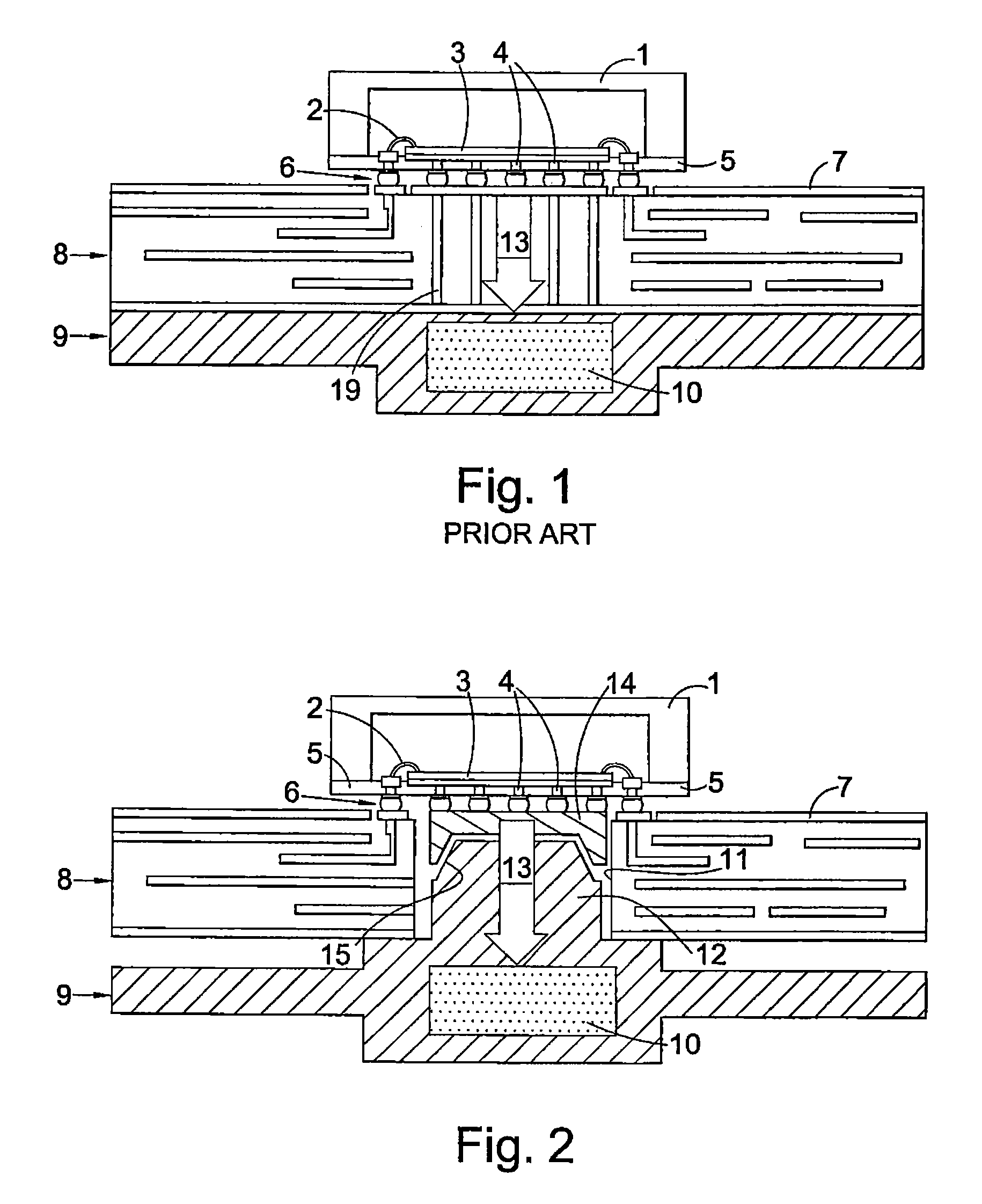
[0014]Corresponding components in the different drawings are given the same reference numerals. As shown in FIG. 1, an hermetically sealed integrated circuit box 1 has for its base a PCB 5 with an array of through-holes 4 to a BGA 6 comprising solder balls, as is well known. A high power integrated circuit, such as a power amplifier 3, is mounted on the PCB 5 and external leads connect it to peripheral interconnection pads on the PCB 5. The BGA 6 is bonded with good electrical and thermal contact to a printed circuit 7 on a PCB 8 which itself is bonded to the upper surface of a metallic girder 9 which acts as a heat sink and conveys heat away from the box 1, through the BGA, to further heat sinks such as exposed fins (not shown). The heat sink 9 has an enclosed channel 10 for a fluid cooling system. Thermal transfer shown by the arrow 13 through the PCB 8 is achieved with the use of narrow vertical channels 19.

[0015]As shown in FIG. 2, the invention provides an improved system for t...


PUM

PropertyMeasurementUnit
power consumptionaaaaaaaaaa
thermally-conductiveaaaaaaaaaa

Abstract

An assembly comprising a first printed circuit board, PCB, with a ball grid array, BGA, on its underside, a second PCB facing the first PCB and having at least one through-hole between its top and bottom surfaces, its top surface printed with a circuit pattern bonded to the BGA, a heat sink layer facing the bottom surface of the second PCB and having at least one thermally-conductive pin projecting normally into the through-hole or a respective one of the through-holes in the second PCB, and, for each pin, a thermally-conductive stud of the same cross-section as the pin, bonded to the BGA and disposed within the through-hole between the pin and the first PCB in thermal contact with the pin.

Description

CROSS-REFERENCE TO RELATED APPLICATION[0001]The present application claims the benefit of British Patent Application No. 0812139.4, filed Jul. 2, 2008, which is hereby incorporated by reference in their entirety.FIELD OF THE INVENTION[0002]This invention relates to a printed circuit board, PCB, assembly and to a method of making such an assembly. It is particularly although not exclusively concerned with the use of a ball grid array, BGA, component as part of the assembly.BACKGROUND OF THE INVENTION[0003]Heat dissipation from printed circuit boards poses a serious problem particularly in the case of high power amplifiers: integrated circuit chips for such amplifiers can for example generate in excess of 3 W each, and for some applications such as antenna arrays with several thousand chips the power consumption can be 30 kW or more. Part of the problem lies in the high level of spatial integration using multiple layers of PCBs, since it becomes difficult to arrange for a short path l...

Claims


Application Information

Patent Timeline
Patent Type & Authority Patents(United States)
IPC IPC(8): H05K1/00H05K3/36
CPCH01L23/473H05K1/0203H01L23/433H01L23/367Y10T29/49126H01L2224/48091H01L2224/48227H01L2924/15311H01L2924/16152H05K3/0061H05K2201/0379H05K2201/09054H05K2201/10734H05K2203/167H01L24/48H01L2924/00014H01L2924/14H01L2924/181H01L2924/00H01L2924/00012H01L2224/45099H01L2224/45015H01L2924/207H05K1/0204
Inventor LOISELET, EMMANUELWILLS, PHIL
Owner THALES HLDG UK
Features
  • R&D
  • Intellectual Property
  • Life Sciences
  • Materials
  • Tech Scout
  • Unparalleled Data Quality
  • Higher Quality Content
  • 60% Fewer Hallucinations
Learn More