
Microlens, microlens array structure and manufacturing process thereof
An array structure and microlens technology, applied in microstructure technology, microstructure devices, manufacturing microstructure devices, etc., can solve the problems of low resolution, crosstalk, incomplete image distinction, etc., to improve resolution, reduce crosstalk, Distinguish obvious effects
Patent Information
- Authority / Receiving Office
- CN · China
- Patent Type
- Applications(China)
- Current Assignee / Owner
- Publication Date
- 2013-11-20
Smart Images
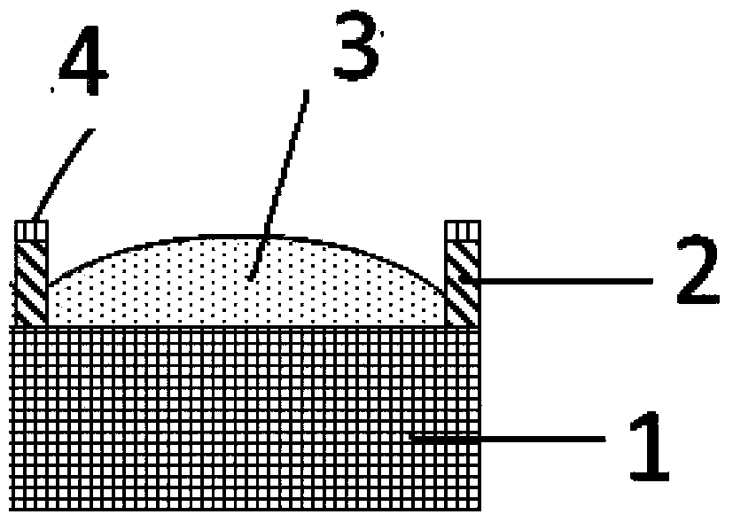
Figure 1 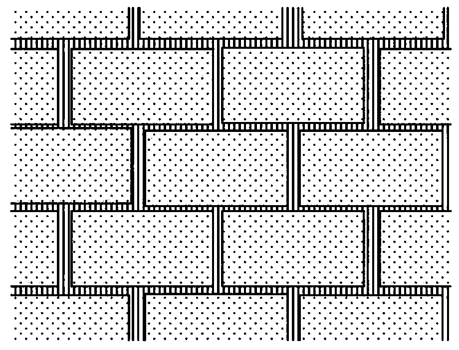
Figure 2 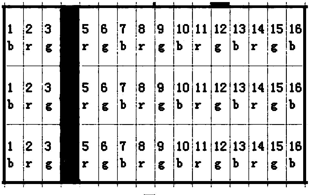
Figure 3
Abstract
Description
technical field
[0001] The invention relates to a subpixel microlens liquid lens array structure, in particular to a subpixel microlens liquid lens array structure after rearranging microlens subimages with red, green and blue subpixels as viewpoints. Background technique
[0002] Integrated imaging technology is becoming more and more mature, but there are still some key technical problems in the current integrated imaging display: in the acquisition process, the preparation of large size, uniform focal length, and large crosstalk is a key technology that restricts integrated imaging stereoscopic display. In the reconstruction process, the true 3D image reconstructed by the microlens array has problems such as small depth of field, narrow viewing angle, and low resolution.
[0003] Existing imaging technologies generally adopt the RGB color mode. RGB is the color representing the three channels of red, green, and blue (hereinafter referred to as RGB). This standard includes...
Examples
Embodiment approach
[0039] Microlens array is an optical device widely used in three-dimensional stereoscopic display. The microlens array is used in the acquisition stage and reproduction stage of integrated imaging, and its size, shape, focal length and other parameters have an important impact on the image display quality. Therefore, the preparation of a microlens array that meets the requirements is very critical for the research of integrated imaging. The manufacturing process of the present invention mainly has five steps. In the manufacturing process, each step requires high precision, so that the manufactured microlens array can have good uniformity and consistent optical characteristics. The method of implementation is as follows:
[0040] (1) Lamination
[0041] Microlens arrays are generally fabricated on glass substrates, first by cleaning the glass substrates and cutting them into required dimensions. Then, the photoresist is pressed on the glass substrate with a lamination machin...