
Solar Cells and Solar Cell Modules
A technology for solar cells and components, applied in the field of solar cells, can solve the problems of high cost of technical steps, and achieve the effect of cheap and easy production
Patent Information
- Authority / Receiving Office
- CN · China
- Patent Type
- Patents(China)
- Current Assignee / Owner
- Publication Date
- 2016-03-09
Smart Images
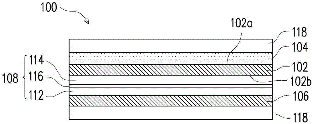
Figure 1 
Figure 2 
Figure 3
Abstract
Description
technical field
[0001] The present invention relates to a solar cell technology, and in particular to a solar cell and a solar cell component. Background technique
[0002] Although the theoretical efficiency of solar cells is high, the actual power generation efficiency is not. There are many factors that affect the efficiency, such as the series and parallel resistance of the solar cell itself, or the shading effect of the solar cell electrodes on the sunlight, or the loss of reflected light that is not effectively captured, and so on.
[0003] The recombination of electrons and holes inside the solar cell is another important factor affecting the efficiency. Absorption of incident photons with energy higher than the band gap of the solar cell generates electron-hole pairs, and then the action of the electric field present at the p-n junction of the solar cell separates these carriers. The photogenerated minority carriers (ie, electrons or holes in electron-hole pairs) w...
Examples
Embodiment Construction
[0085] figure 1 is a schematic diagram of a solar cell according to the first embodiment of the present invention.
[0086] exist figure 1 Shown in is a solar cell 100, which at least includes a first electrode 102 having an outer surface 102a and an inner surface 102b, a second electrode 106 having an outer surface and an inner surface, an inner surface 102b located on the first electrode 102, and a second electrode 106 The photoelectric conversion layer 108 between the inner surfaces. The solar cell 100 further includes an ionizable charged film (ionizable charged film) 104 located on at least one of the outer surface 102 a of the first electrode 102 and the outer surface of the second electrode 106 . The photoelectric conversion layer 108 may include a semiconductor base region 112 , a semiconductor emitter region 114 and a p-n junction region 116 , wherein the p-n junction region 116 is located between the semiconductor base region 112 and the semiconductor emitter regio...