
A single photon avalanche diode with high detection efficiency and its manufacturing method
A single-photon avalanche and detection efficiency technology, applied in the field of single-photon detection, can solve the problems of low detection sensitivity and photon detection efficiency, and achieve the effects of increasing light transmittance, increasing width, and uniform electric field
Patent Information
- Authority / Receiving Office
- CN · China
- Patent Type
- Patents(China)
- Current Assignee / Owner
- Publication Date
- 2020-01-21
Smart Images
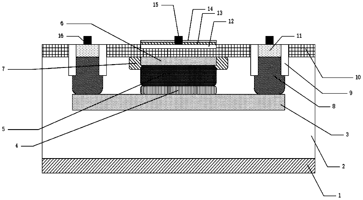
Figure 1
Abstract
Description
technical field
[0001] The invention belongs to the technical field of single photon detection, and in particular relates to a single photon avalanche diode with high detection efficiency and a manufacturing method thereof. Background technique
[0002] Single-photon detection technology is a very low-light detection and sensing technology, which has been widely used in contemporary life, such as in bioluminescence, quantum communication, astronomical research, and high-sensitivity sensors. As the core device of single photon detection, the single photon avalanche diode based on CMOS technology has attracted more and more attention and attention of researchers. Among them, the photon detection efficiency (Photon Detection Efficiency, PDE) is a key factor to measure the single photon detection ability of the avalanche photodiode. Therefore, designing a device structure with high photon detection efficiency is of great significance and use value.
[0003] The traditional sin...
Examples
Embodiment Construction
[0032] The present invention will be further described below in conjunction with accompanying drawing.
[0033] Such as figure 1 As shown, the single photon avalanche diode with high detection efficiency includes coaxially arranged p-substrate layer 1, p epitaxial layer 2, n+ buried layer 3, n-type charge layer 4, inversion deep n well 5, p-type charge layer 6. P-type semiconductor layer 7, n well layer 8, shallow trench isolation layer 9, p-type semiconductor layer 10, n+ type semiconductor layer 11, p+ type light absorbing layer 12, silicon dioxide anti-reflection film 13, nitrided Silicon antireflection film 14 , anode electrode 15 and cathode electrode 16 .
[0034] The p-substrate layer 1 is arranged at the bottom of the p-epitaxial layer 2 . A disk-shaped n+ buried layer 3 is provided inside the p epitaxial layer 2 . An n-type charge layer 4 , an inversion deep n well 5 , a p-type charge layer 6 , a p-type semiconductor layer 7 and an n-well layer 8 are arranged betwe...