
Imaging Method and Apparatus
a technology of image detection and refraction, applied in the direction of refraction control devices, instruments, radiography, etc., can solve the problem of largely unconstrained number, achieve high photon detection efficiency, reduce intrinsic noise, and maximise the effect of dynamic rang
Patent Information
- Authority / Receiving Office
- US · United States
- Patent Type
- Applications(United States)
- Current Assignee / Owner
- Publication Date
- 2021-04-29
- Estimated Expiration
- Not applicable · inactive patent
Smart Images
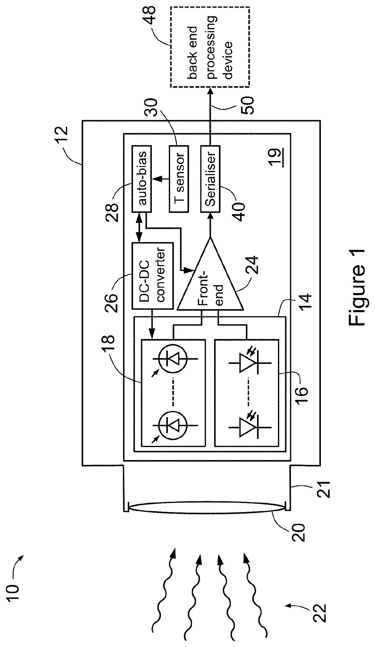
Figure 1 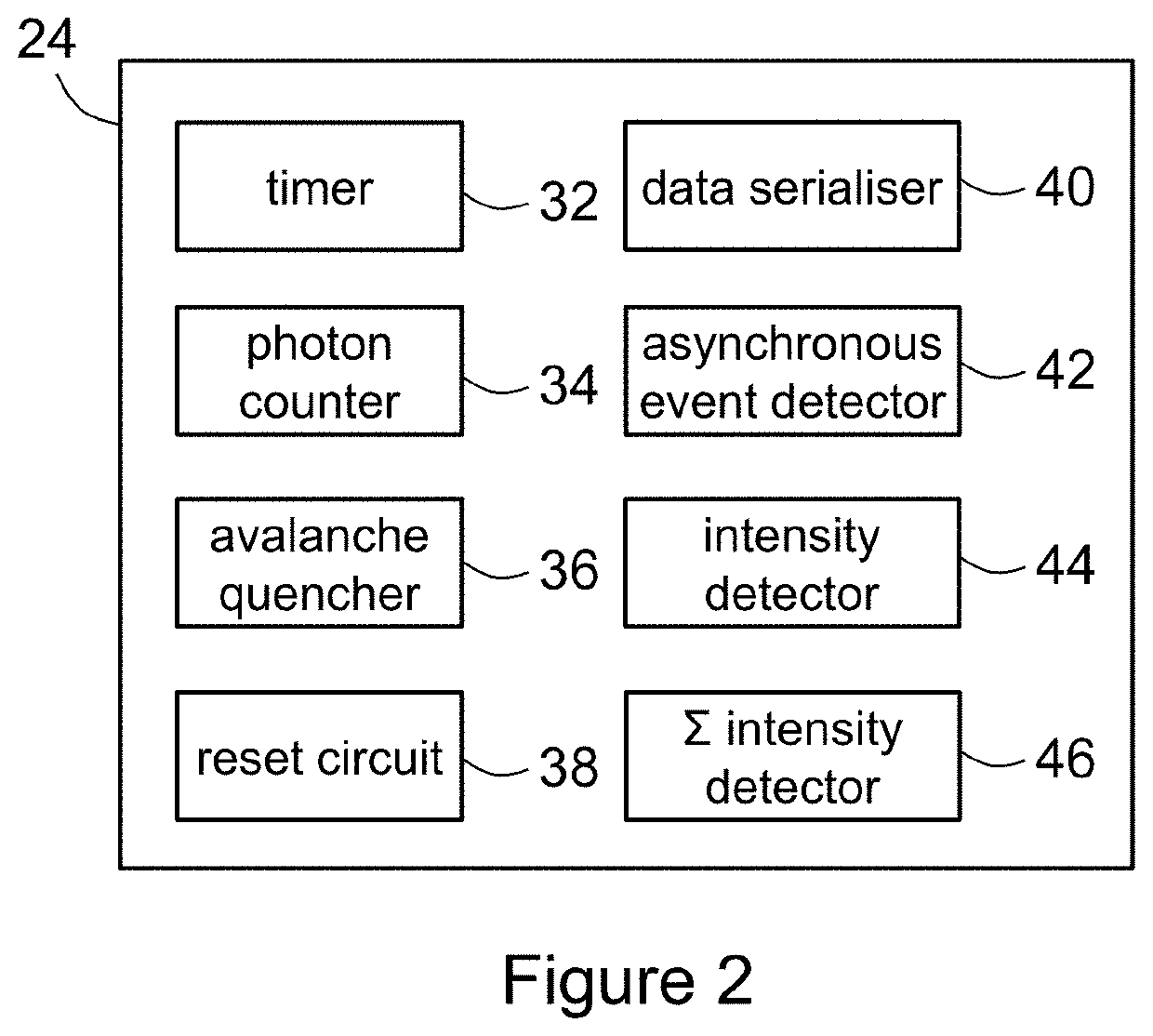
Figure 2 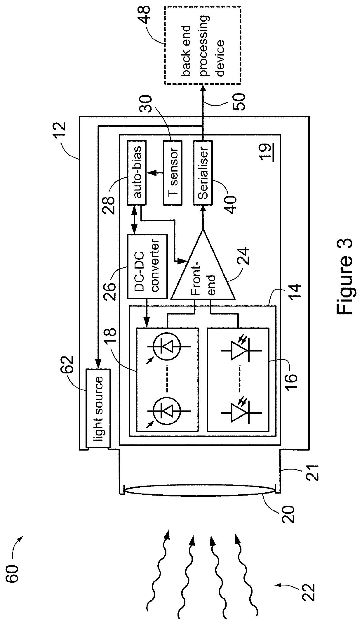
Figure 3
Abstract
Description
FIELD OF THE INVENTION
[0001] The invention relates to an imaging method and apparatus, of particular but by no means exclusive application as a camera for acquiring hyperspectral 3D images.BACKGROUND OF THE INVENTION
[0002] Vision sensors for capturing real time three-dimensional (3D) images form the basis of machine learning systems. Autonomous systems require low latency visual data to maximise their performance particularly in urban environments. Micro unmanned aircraft systems (UASs) require sophisticated simultaneous localisation and mapping (SLAM) systems to navigate safely and are severely payload restricted. A monolithic image sensor capable of operating in these environments with increased observational capabilities is desirable to increase system performance and keep weight, power consumption and total system size to a minimum.
[0003] Single Photon Avalanche Diodes (SPADs) implemented in standard CMOS processes have attracted attention in recent years. High performance SPAD ima...
Examples
Embodiment Construction
[0104]FIG. 1 is a schematic view of a camera 10 for acquiring hyperspectral 3D images according to an embodiment of the invention. Camera 10 includes a housing 12 and an integrated array 14 of photodiodes 16 and SPADs 18, mounted on a die 19 within housing 12. Camera 10 includes a lens train of one or more lenses 20 in a lens unit 21 mounted to housing 12. Lens unit 21 may be detachable from housing 12. Lenses 20 focus incident light 22 to an image on array 14 for detection by array 14.
[0105]In this embodiment, SPADs 18 have a 10 μm diameter sensitive area, a total sensor size of 30 μm×30 μm, and a fill factor of 26%. With the respective front-end circuit, this size becomes 40 μm×60 μm with a fill of factor 3.3%. SPADs 18 have an effective sensitivity from 400 nm to 1000 nm, and a peak sensitivity at 532 nm.
[0106]SPADs and photodiodes in silicon are sensitive in the wavelength range of approximately 190 nm to 1100 nm, that is, from UV to IR. In other semiconductors, such as HgCdTe, ...