
Double-protection ring and forming method thereof
A double protection and protection ring technology, applied in electrical components, circuits, semiconductor devices, etc., can solve the problem that the effect of suppressing the latch-up effect needs to be improved.
Patent Information
- Authority / Receiving Office
- CN · China
- Current Assignee / Owner
- Publication Date
- 2019-03-29
Smart Images
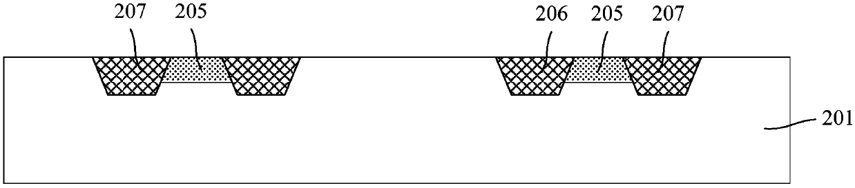
Figure 1 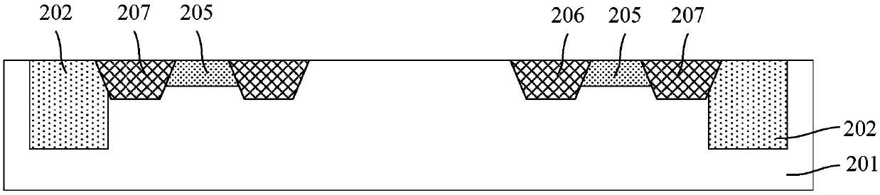
Figure 2 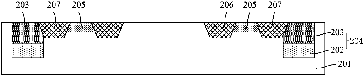
Figure 3
Abstract
Description
technical field
[0001] The invention relates to the field of semiconductor manufacturing, in particular to a double protection ring and a forming method thereof. Background technique
[0002] The latch-up effect is a self-destructive phenomenon in which the parasitic thyristor (SCR) of the complementary MOS field effect transistor (CMOS) is turned on by the pulse current or voltage fluctuation, resulting in the amplification effect of the avalanche current. The establishment of a low-impedance path between the Vdd (power supply voltage) and Vss (ground voltage) power lines can allow high currents to flow between parasitic circuits, causing the circuits to stop working properly or even self-destruct.
[0003] In the prior art, the resistance value can be reduced by means of reverse doping wells, trench isolation, and adding an epitaxial layer on the heavily doped substrate, so as to achieve the effect of suppressing parasitic effects.
[0004] For devices with a smaller proc...
Examples
Embodiment Construction
[0028] As mentioned in the background art, the suppression effect of the existing guard ring on the latch-up effect still needs to be improved.
[0029] Research has found that the junction depth of the existing guard ring is shallow, and its ability to absorb substrate charges is limited, so that the guard ring has a limited suppression effect on the latch-up effect. Although the suppression effect can be enhanced by increasing the number of guard rings, too many guard rings will increase the area of the chip and noises will crosstalk each other.
[0030] To this end, an embodiment of the present invention provides a guard ring and a method for forming the guard ring. In the guard ring formation method, an N-type second guard ring is formed in a P-type substrate, and the N-type second guard ring is formed in a P-type substrate. The guard ring includes an N-type first well region and an N-type second well region deeper than the N-type first well region, so that the N-type se...