
An extremely low reverse recovery charge superjunction power vdmos
A technology of reverse recovery charge and power, applied in circuits, electrical components, electric solid-state devices, etc., can solve problems such as improving the reverse recovery characteristics of SJ-VDMOS body diodes, the level of limited freewheeling current, and the increase of leakage current , to achieve excellent reverse recovery characteristics, improve reverse recovery characteristics, and reduce the effect of Qrr
Patent Information
- Authority / Receiving Office
- CN · China
- Patent Type
- Patents(China)
- Current Assignee / Owner
- Publication Date
- 2020-12-11
Smart Images
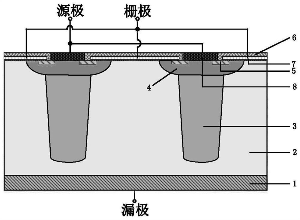
Figure 1 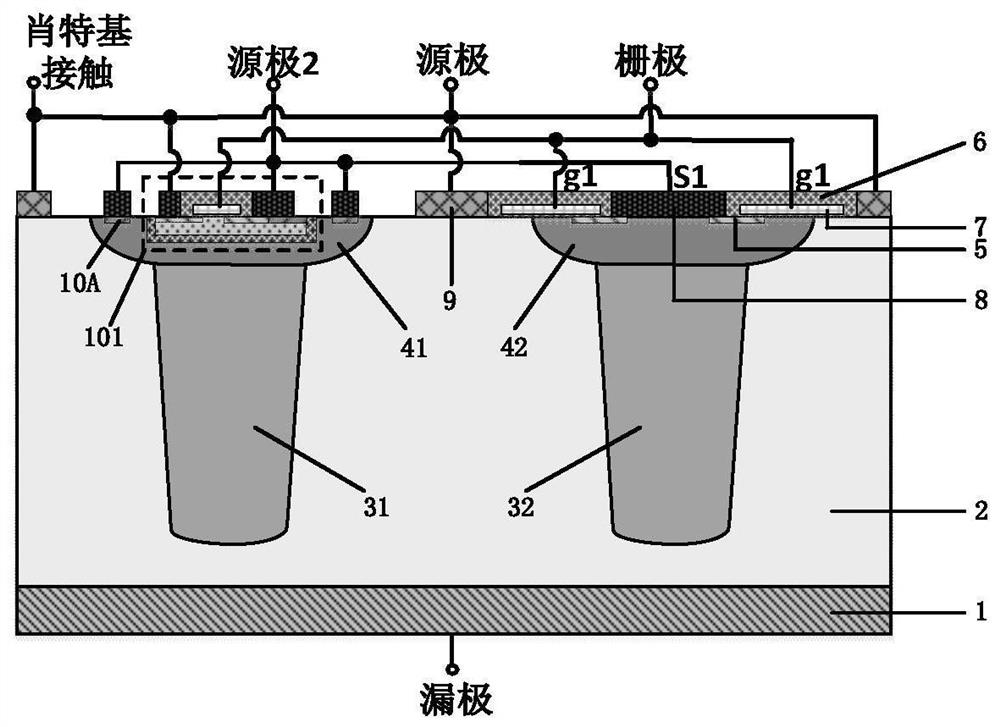
Figure 2 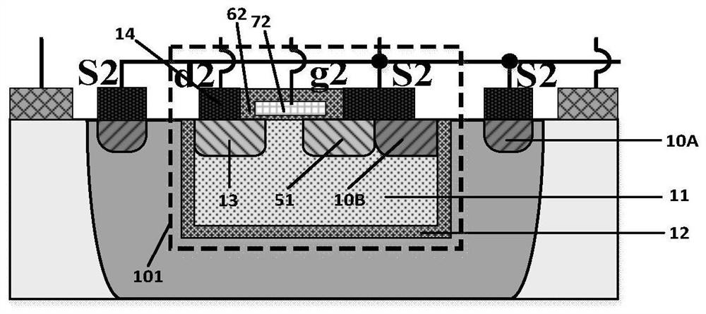
Figure 3
Abstract
Description
technical field
[0001] The invention relates to the field of power semiconductor devices, in particular to a preparation method of a super junction power VDMOS device with extremely low reverse recovery charge Background technique
[0002] Super Junction Vertical Double-diffusion Metal-oxide-semiconductor (SJ-VDMOS for short) breaks the limit of silicon, achieves extremely low on-resistance while maintaining high endurance of the device The voltage performance makes it widely used in pulse width modulation and motor control circuits.
[0003] Traditional SJ-VDMOS introduces highly doped P-columns to deplete each other laterally with the high-concentration N-type withstand voltage layer to reduce the vertical electric field of the device and achieve high withstand voltage capability and low on-resistance of the device. However, the highly doped p-column greatly improves the anode emission area and hole injection efficiency of the SJ-VDMOS body diode, resulting in extremely p...
Examples
Embodiment Construction
[0022] An extremely low reverse recovery charge superjunction power VDMOS, including a superjunction VDMOS, the superjunction VDMOS includes an N-type substrate 1 that doubles as a drain and an N-type drift region 2 disposed on the N-type substrate 1 , which is characterized in that a first P column 31 is provided in the N-type drift region 2 of the super junction VDMOS, and a first P-type body region 41 is provided on the top of the first P column 31, and the first P-type body region 41 The top surface is flush with the top surface of the N-type drift region 2, an N MOS transistor 101 is arranged on the first P-type body region 41, and an NMOS transistor 101 is arranged between the N MOS transistor 101 and the first P-type body region 41. With SiO 2 The isolation layer 12 is further provided with a first P-type heavily doped region 10A on the first P-type body region 41, the source metal of the super junction VDMOS, the source metal of the N MOS transistor 101 and the first P...