
Rapid superjunction longitudinal double-diffusion metal oxide semiconductor transistor
A technology of vertical double-diffusion and semiconductor tubes, which is applied in the direction of semiconductor devices, electrical components, circuits, etc., can solve the problems of large reverse recovery charges, increased junction area, and restrictions on the reverse recovery characteristics of devices, so as to improve the lateral withstand voltage Level, the effect of improving the pressure resistance performance
Patent Information
- Authority / Receiving Office
- CN · China
- Patent Type
- Patents(China)
- Current Assignee / Owner
- Publication Date
- 2012-06-13
- Estimated Expiration
- Not applicable · inactive patent
Smart Images
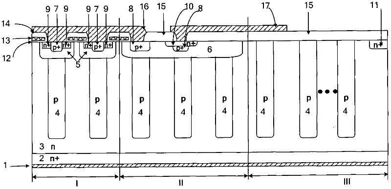
Figure 1 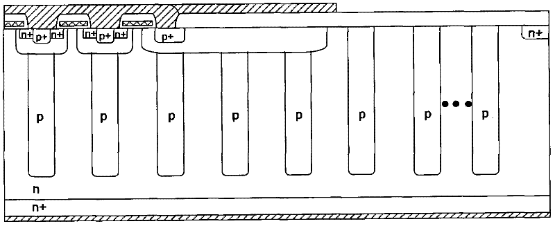
Figure 2 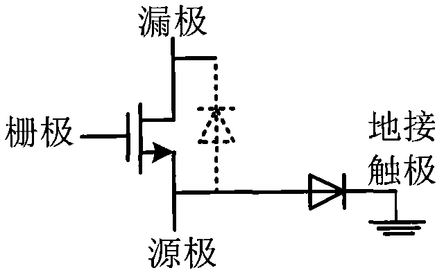
Figure 3
Abstract
Description
technical field
[0001] The invention relates to a high-voltage power metal oxide semiconductor device made of silicon, more precisely, a high-voltage superjunction vertical double-diffused metal oxide semiconductor field effect transistor made of silicon. Background technique
[0002] At present, power devices are more and more widely used in daily life, production and other fields, especially power metal oxide semiconductor field effect transistors, because they have faster switching speed, smaller drive current, and wider safe operating area , so it has been favored by many researchers. Nowadays, power devices are developing rapidly in the direction of increasing operating voltage, increasing operating current, reducing on-resistance and integration. Among many power MOSFET devices, especially in vertical power MOSFETs, the invention of super junction semiconductor power devices overcomes the on-resistance of traditional power MOSFETs The contradiction between the breakd...
Examples
Embodiment Construction
[0023] refer to figure 1 , a fast superjunction vertical double-diffused metal oxide semiconductor tube, comprising: a cell region I, a terminal region III located on the outermost periphery of the chip, and a transition region II between the cell region I and the terminal region III, in the cell region A drain metal 1 is provided at the bottom of the cell region I, transition region II and terminal region III, and a heavily doped n-type silicon substrate 2 is arranged on the drain metal 1 as the drain region of the chip. An n-type doped epitaxial layer 3 is arranged on the n-type silicon substrate 2, and a discontinuous p-type doped columnar semiconductor region 4 is arranged in the n-type doped epitaxial layer 3,
[0024] A first p-type doped semiconductor region 5 is provided on the p-type doped columnar semiconductor region 4 in the cell region 1, and the first p-type doped semiconductor region 5 is located in the n-type doped epitaxial layer 3. A p-type doped semiconduc...