
Nonvolatile Boolean logic operation unit, method and device
A technology of Boolean logic and operation unit, applied in electrical components, instruments, electrical digital data processing, etc.
Patent Information
- Authority / Receiving Office
- CN · China
- Current Assignee / Owner
- Publication Date
- 2020-12-01
Smart Images
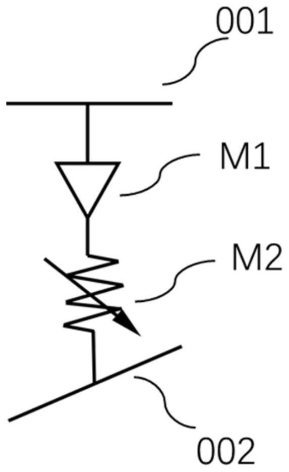
Figure 1 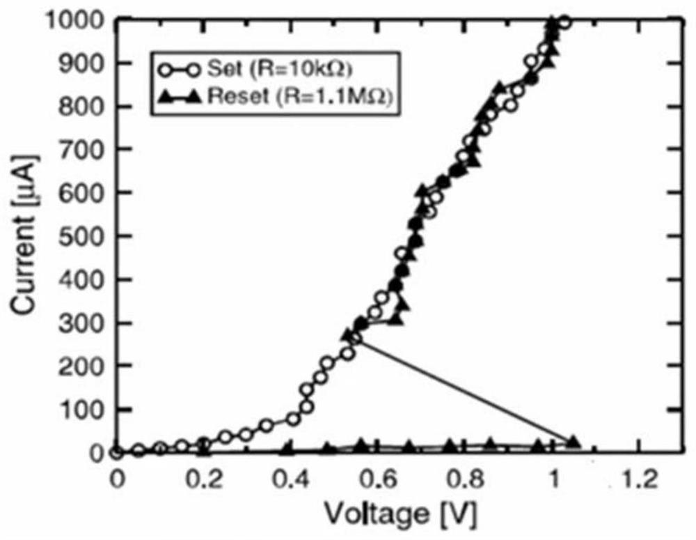
Figure 2 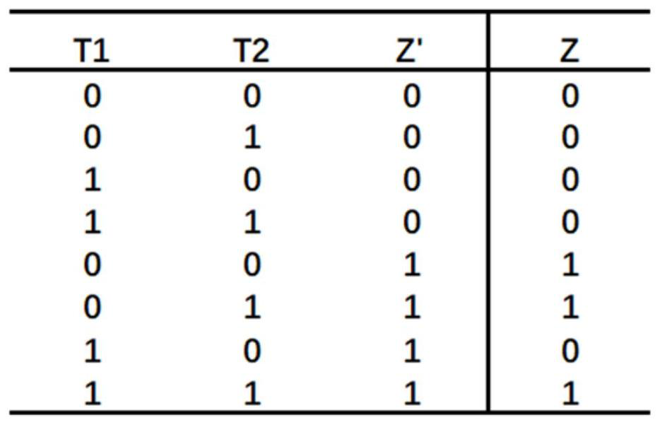
Figure 3
Abstract
Description
technical field
[0001] The invention relates to the field of semiconductor devices, in particular to a nonvolatile Boolean logic operation unit, method and device. Background technique
[0002] Traditional computer operations are based on the von Neumann architecture. In this structure, computing and storage are two completely separate units. The computing unit reads data from the memory and calculates according to the instructions. After completing the calculation and processing, it returns to the memory for storage. The rapid development of information technology has brought the computer field into a data-centric era of big data. The explosive growth of data scale and the separation of storage and computing architecture make the computing speed slower and slower, resulting in storage walls and data computing. Energy efficiency ratio bottleneck problem. In order to solve this problem, constructing a phase-change memory non-volatile logic operation method that integrates co...
Examples
Embodiment Construction
[0049] The present invention will be described in detail below in conjunction with the accompanying drawings and specific embodiments. This embodiment is carried out on the premise of the technical solution of the present invention, and detailed implementation and specific operation process are given, but the protection scope of the present invention is not limited to the following embodiments.
[0050] A nonvolatile Boolean logic operation unit such as figure 1 As shown, it includes a diode M1 and a phase-change memory unit M2, the anode of the diode M1 is used as the first pulse signal input terminal 001 to receive the first pulse signal, the cathode is connected to one end of the phase-change memory unit M2, and the other end of the phase-change memory unit M2 The second pulse signal is received as the second pulse signal input terminal 002 .
[0051] The resistance value of the phase change memory is used to represent the logic state "0" and "1", which is different from t...