
Power Semiconductor Module
a technology of semiconductor modules and semiconductor components, applied in the direction of printed circuit manufacturing, printed circuit aspects, laminated printed circuit boards, etc., can solve the problems of device damage or device characteristics degradation, difficulty in making the coefficient of thermal expansion of materials above and below the device equal, and fracture of the joining part, so as to prevent the fracture of the joining parts, reduce the possibility of device damage, and reduce the effect of pressur
Patent Information
- Authority / Receiving Office
- US · United States
- Patent Type
- Applications(United States)
- Current Assignee / Owner
- Publication Date
- 2007-11-22
- Estimated Expiration
- Not applicable · inactive patent
Smart Images
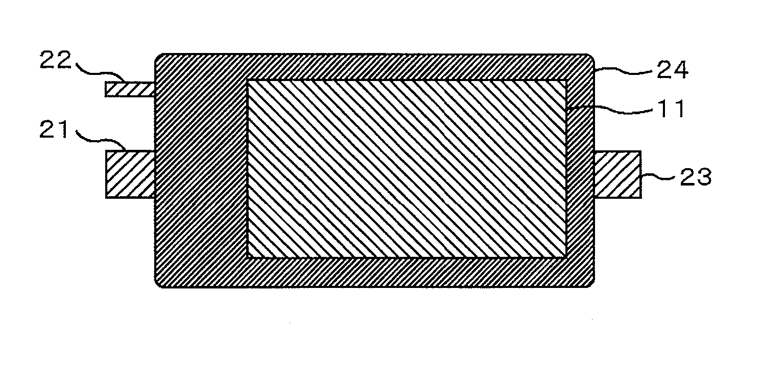
Figure 1 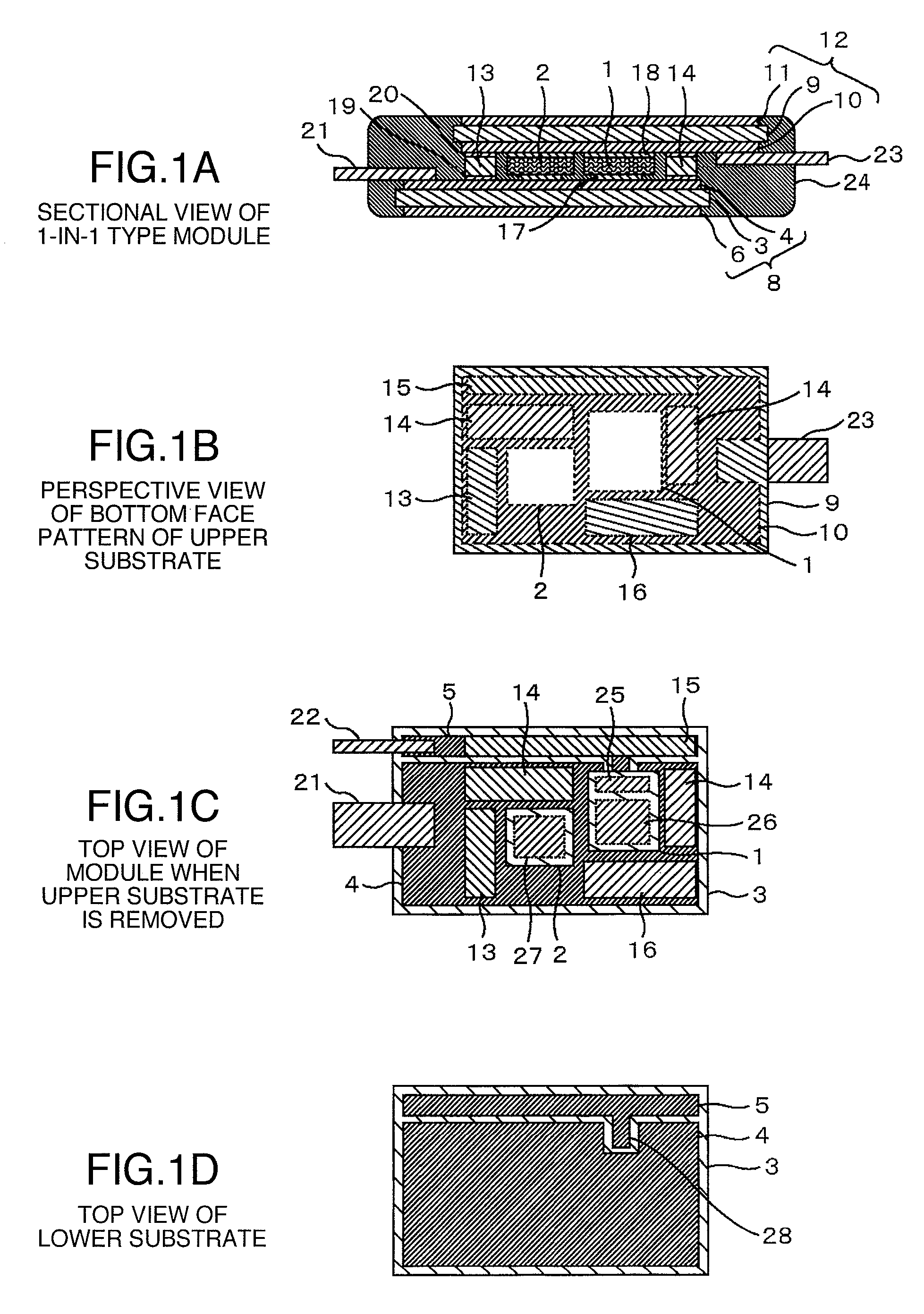
Figure 2 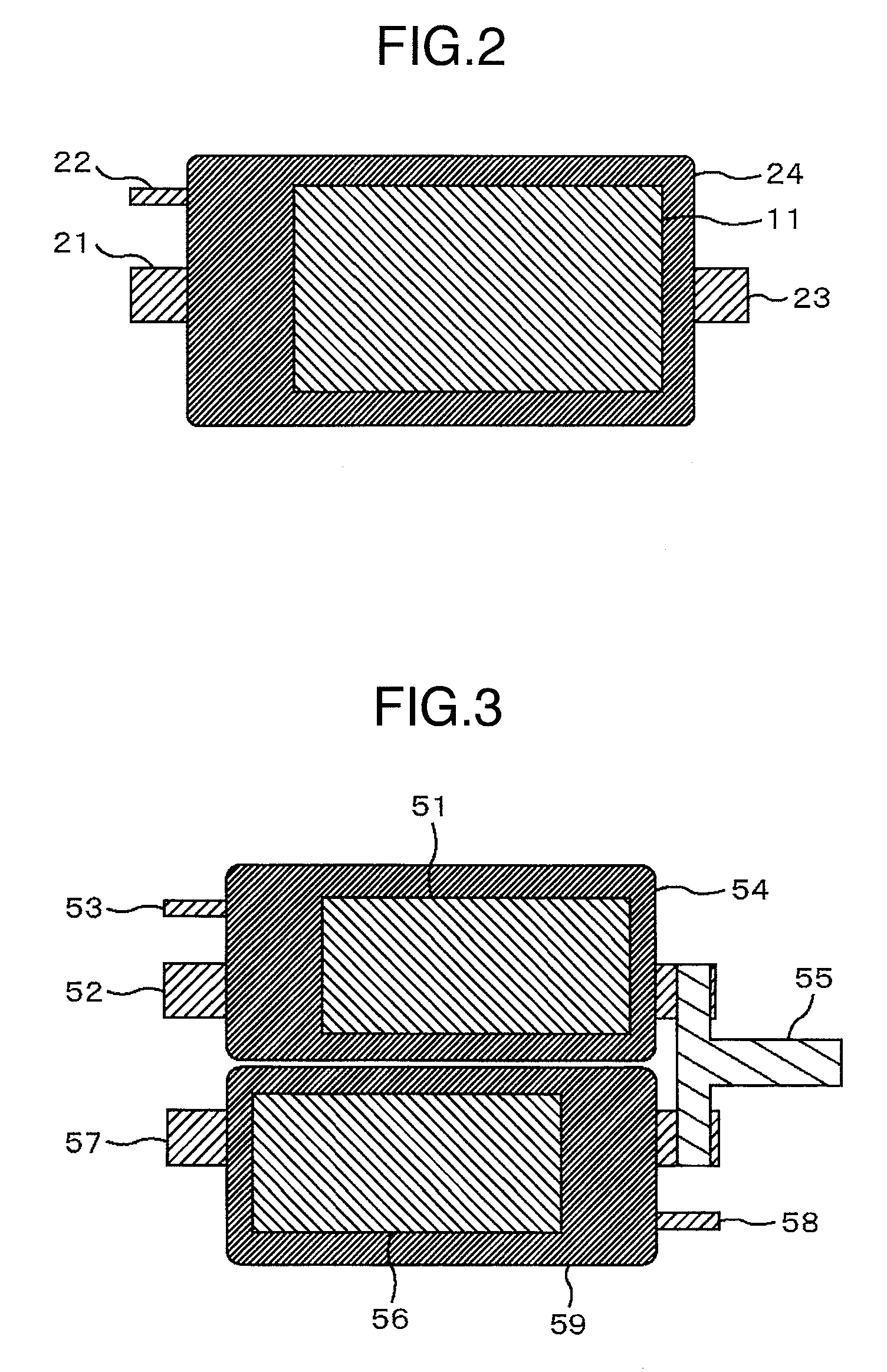
Figure 3
Abstract
Description
BACKGROUND OF THE INVENTION
[0001] The present invention relates to a large current control semiconductor device used in high temperature environments represented by use in automobiles. In particular, the present invention relates to a power semiconductor module that is excellent in heat resistance of its junction and constituent materials and excellent in thermal fatigue life against the thermal cycling test or the power cycling test caused by the on / off of the device, even in the case where operation is conducted with the junction temperature of the semiconductor device in the range of 175 to 250° C.
[0002] Power semiconductor modules including power devices, such as MOSFETs and IGBTs, for exercising switching control on a large current and diodes for releasing the reverse voltage generated at the time of switching are used in wide fields ranging from household electric appliances to vehicles as main components of inverter apparatuses for power converter. In recent years, motor contro...
Examples
Embodiment Construction
[0025]Hereafter, embodiments of the present invention will be described in detail with reference to the drawings.
[0026]FIGS. 1A-1D show an embodiment of a power semiconductor module according to the present invention including one power transistor device and one diode device. FIG. 1A is a sectional view of the module. FIG. 1B is a perspective view of a metal electrode of a device side face on an upper ceramic substrate with printed circuit. FIG. 1C is a top view obtained when an upper substrate with printed circuit and resin are removed. FIG. 1D is a top view of a lower substrate with printed circuit. In FIGS. 1A-1D, an IGBT chip 1 and a diode chip 2 are joined onto a ceramic substrate with printed circuit 8 having metal electrodes 4, 5 and 6 of Cu formed above and below a low thermal expansion ceramic substrate 3 with printed circuit, by high temperature solder 17 having a temperature at solidus line of at least 260° C. formed of SnSbAgCu. Electroless Ni—P plating having a thicknes...