
Printed circuit board and method of manufacturing the same
a printed circuit board and manufacturing method technology, applied in the direction of printed circuit aspects, non-metallic protective coating applications, conductive pattern formation, etc., can solve the problems of reducing the reliability of printed circuit boards, increasing manufacturing costs, and prolonging lead time, so as to achieve simple performance and minimize the separation of circuit layers
Patent Information
- Authority / Receiving Office
- US · United States
- Patent Type
- Applications(United States)
- Current Assignee / Owner
- Publication Date
- 2011-04-21
Smart Images
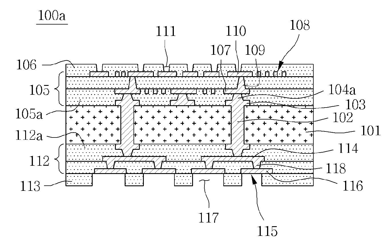
Figure 1 
Figure 2 
Figure 3
Abstract
Description
CROSS REFERENCE TO RELATED APPLICATION
[0001] This application claims the benefit of Korean Patent Application No. 10-2009-0099869, filed Oct. 20, 2009, entitled “A printed circuit board and a fabricating method the same”, which is hereby incorporated by reference in its entirety into this application.BACKGROUND OF THE INVENTION
[0002] 1. Technical Field
[0003] The present invention relates to a printed circuit board and a method of manufacturing the same.
[0004] 2. Description of the Related Art
[0005] Recently, in order to cope with an increase both in signal transmission speed and density of semiconductor chips, the demand for techniques for directly mounting a semiconductor chip on a PCB is increasing. Thus, the development of a PCB having high density and high reliability capable of coping with the increasing density of the semiconductor chip is required.
[0006] The requirements for the PCB having high density and high reliability are closely related to the specs of the semiconductor chip,...
Examples
first embodiment
[0054]FIG. 8 is a cross-sectional view of a printed circuit board 100a according to the present invention. With reference to the drawing, the printed circuit board 100a according to this embodiment of the invention is described below.
[0055]As shown in FIG. 8, the printed circuit board 100a according to this embodiment is configured such that a core substrate 101, which has through-hole parts 102 and core circuit layers 103 formed on both sides thereof, is provided on one side thereof with a first build-up layer 105 and a first protective layer 106 and is provided on the other side thereof with a second build-up layer 112 and a second protective layer 113, and the outermost circuit layer of the first build-up layer 105 is embodied as a trench circuit layer 108 that is formed using a trench technology.
[0056]Although each of the first build-up layer 105 and the second build-up layer 112 is shown in FIG. 8 as being composed of two layers, it is provided only for illustrative purposes an...
second embodiment
[0076]The bumps 104a may be formed by a metal plating layer or electroconductive metal paste. In this embodiment, the bumps 104a are described as being formed by a metal plating layer, and are described as being formed by electroconductive metal paste in a
[0077]The bumps 104a are provided for forming the electrical connection between the core circuit layer 103 and the innermost circuit layer 107 of the first build-up layer 105 (to be described later) as well as for the electrical connection between the core circuit layer 103 and the innermost circuit layer 114 of the second build-up layer 112. The bumps 104a are configured to protrude from the circuit layer 103. The bumps 104a may be integrally formed along with the core circuit layers 103 by executing a plating process once, or may be separately formed by executing a plating process after formation of the core circuit layers 103. The process of forming the bumps 104a is not limited to the above-mentioned processes but may be formed...