
Semiconductor laser device
a laser device and semiconductor technology, applied in the direction of lasers, semiconductor lasers, laser optical resonators, etc., can solve the problems of limited application of conventional dfb lasers to light sources for optical communication over a relatively short distance and at a relatively low transmission speed, and achieve the effect of low refractive index
Patent Information
- Authority / Receiving Office
- US · United States
- Patent Type
- Applications(United States)
- Current Assignee / Owner
- Publication Date
- 2012-01-26
- Estimated Expiration
- Not applicable · inactive patent
Smart Images
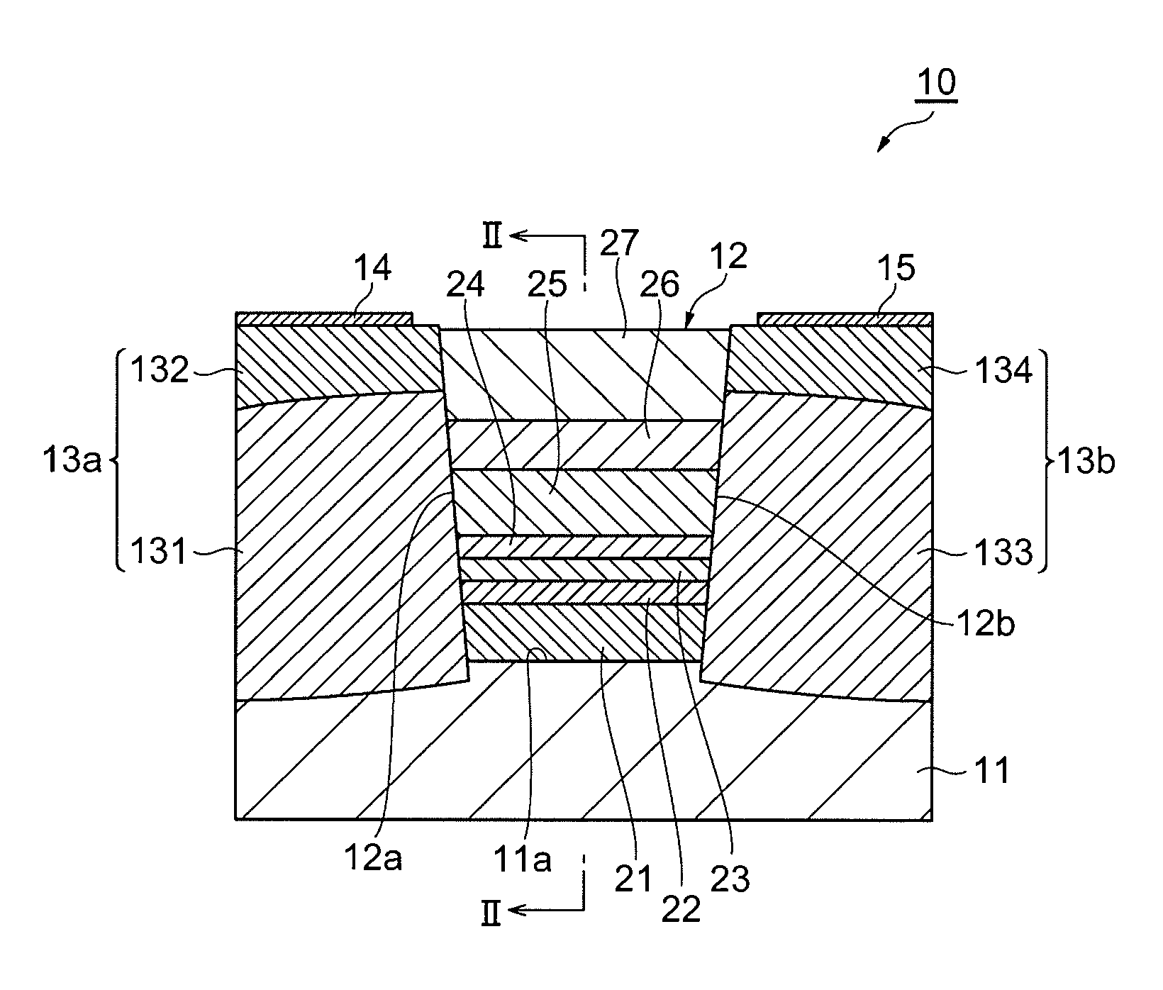
Figure 1 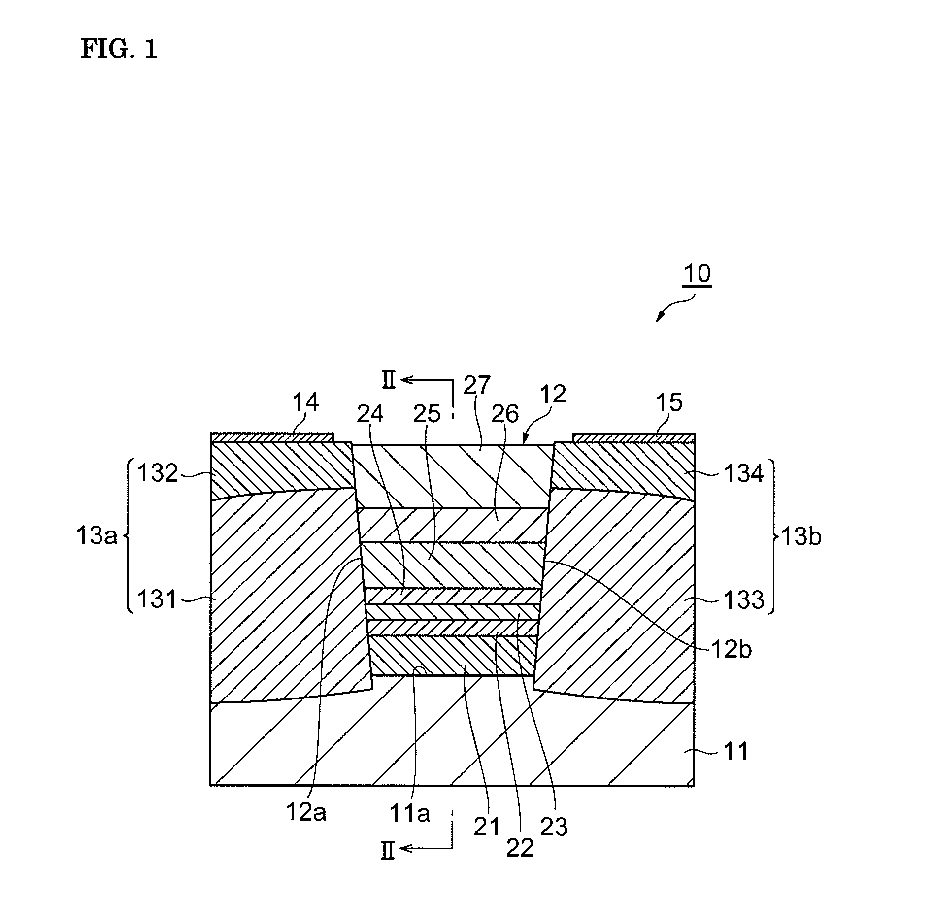
Figure 2 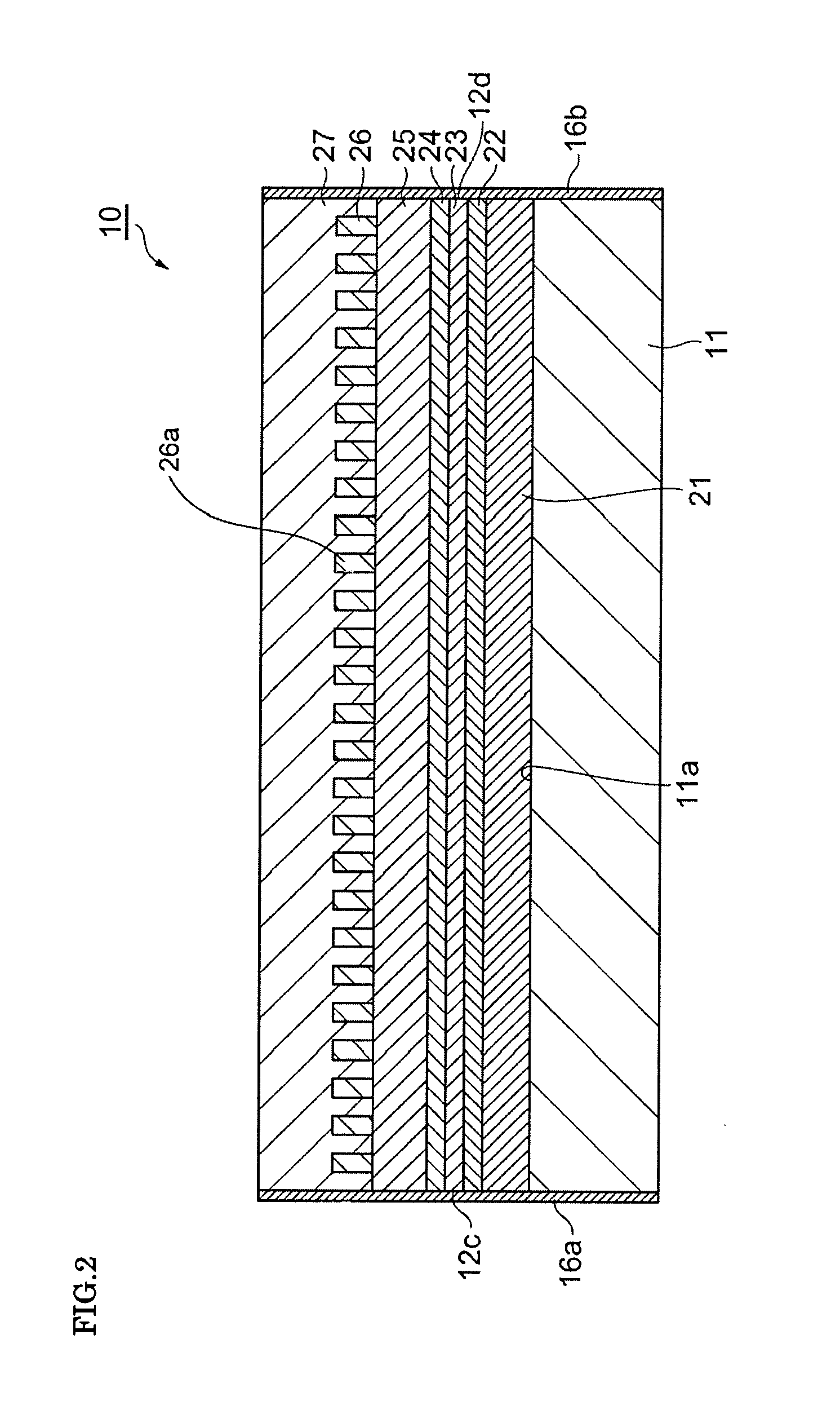
Figure 3
Abstract
Description
BACKGROUND OF THE INVENTION
[0001] 1. Field of the Invention
[0002] The present invention relates to a semiconductor laser device.
[0003] 2. Description of the Related Art
[0004] Patent Document 1 (Japanese Unexamined Patent Application Publication No. 7-249829) describes a distributed feedback laser (DFB laser) formed on a semiconductor substrate. This DFB laser includes a p-type InP cladding layer, an optical guide layer, an active layer having a strained quantum well structure, and an n-type InP cladding layer. These layers are stacked on a p-type InP substrate in this order. A diffraction grating is formed at the interface between the p-type InP cladding layer and the optical guide layer. The p-type InP cladding layer and the n-type InP cladding layer have smaller refractive indices than the optical guide layer and the active layer. Specifically, the DFB laser has a single optical-waveguide structure constituted by the p-type InP cladding layer, the optical guide layer, the active layer...
Examples
first embodiment
[0023]FIG. 1 is a sectional view illustrating the structure of a semiconductor laser device 10 according to an embodiment of the present invention. The section illustrated in FIG. 1 is perpendicular to the light propagation direction of the semiconductor laser device 10. FIG. 2 illustrates a section taken along line II-II of FIG. 1. The semiconductor laser device 10 includes a substrate 11, a mesa part 12, buried parts 13a and 13b, an anode electrode 15, and a cathode electrode 14. The mesa part 12 is disposed on the substrate 11. The buried parts 13a and 13b are disposed on the substrate 11 and on the lateral surfaces of the mesa part 12. The mesa part 12 is buried with the buried parts 13a and 13b.
[0024]The substrate 11 has a main surface 11a. In the first embodiment, a III-V group compound semiconductor such as InP is epitaxially grown on the main surface 11a. The substrate 11 is preferably composed of a semi-insulating semiconductor. For example, the substrate 11 is made of Fe-...