
Semiconductor device and production method for semiconductor device
Patent Information
- Authority / Receiving Office
- US · United States
- Current Assignee / Owner
- Publication Date
- 2015-01-15
- Estimated Expiration
- Not applicable · inactive patent
Smart Images
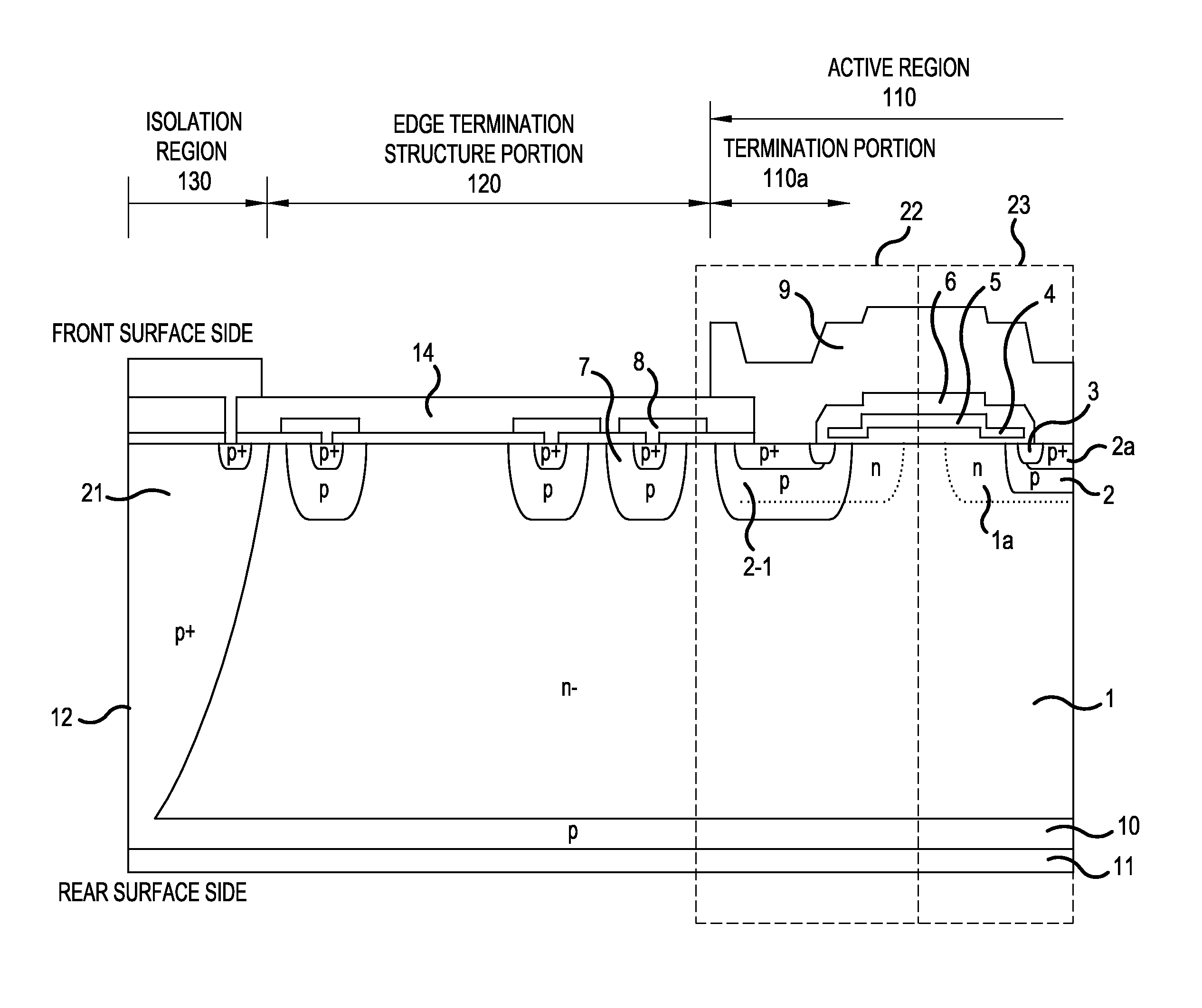
Figure 1 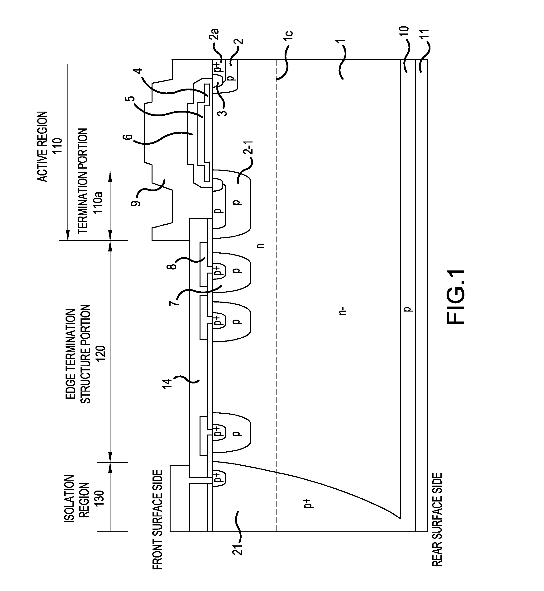
Figure 2 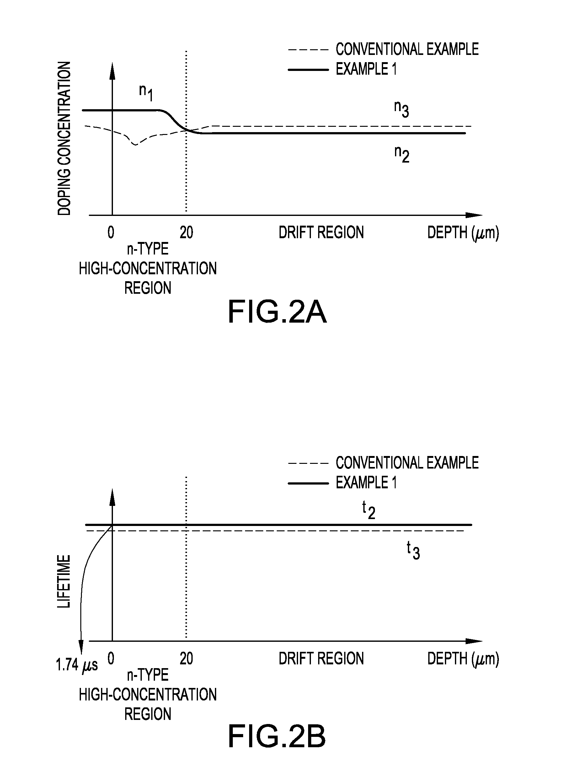
Figure 3
Abstract
Description
BACKGROUND OF THE INVENTION
[0001] A. Field of the Invention
[0002] The present invention relates to a reverse blocking IGBT which can improve a trade-off relationship among a reverse leakage current at a reverse breakdown voltage, an on-state voltage, and switching loss and a method for producing the same.
[0003] B. Description of the Related Art
[0004] A high-breakdown-voltage discrete power device plays a key role in a power conversion device. Examples of the power device include an insulated gate bipolar transistor (IGBT) and a MOS gate (metal-oxide-semiconductor insulated gate) field effect transistor (MOSFET). The IGBT is a conductivity-modulation-type bipolar device and has a lower on-state voltage than the MOSFET which is a unipolar device. Therefore, in general, the IGBT is particularly applied to a high-breakdown voltage device for switching in which the on-state voltage is likely to be high.
[0005] When a matrix converter with high conversion efficiency is used as the power convers...
Examples
embodiment
[0040]A reverse blocking IGBT will be described as an example of a reverse blocking semiconductor device according to an embodiment of the invention. FIG. 1 is a cross-sectional view illustrating the structure of a main portion of the reverse blocking IGBT according to the embodiment of the invention. As illustrated in FIG. 1, the reverse blocking IGBT according to the embodiment includes an active region 110 which is provided in the vicinity of the center of a chip, an edge termination structure portion 120 which is provided in the outer circumference surrounding the active region 110, and a isolation region 130 which surrounds the outside of the edge termination structure portion 120. The isolation region 130 includes, as a main region, a p+ isolation layer 21 for connecting one main surface and the other main surface of an n− semiconductor substrate with a p-type region. That is, the p+ isolation layer 21 is provided so as to pass through the n− semiconductor substrate in a depth...