
Optical phase modulator
a phase modulator and optical phase technology, applied in non-linear optics, instruments, optics, etc., can solve the problems of inability to apply control of chirp quantity, weak electrical field confinement, and weak radio frequency characteristic, so as to promote impedance matching, increase the characteristic impedance of the electrode, and increase the operation stability
Patent Information
- Authority / Receiving Office
- US · United States
- Patent Type
- Patents(United States)
- Current Assignee / Owner
- Publication Date
- 2011-01-11
Smart Images
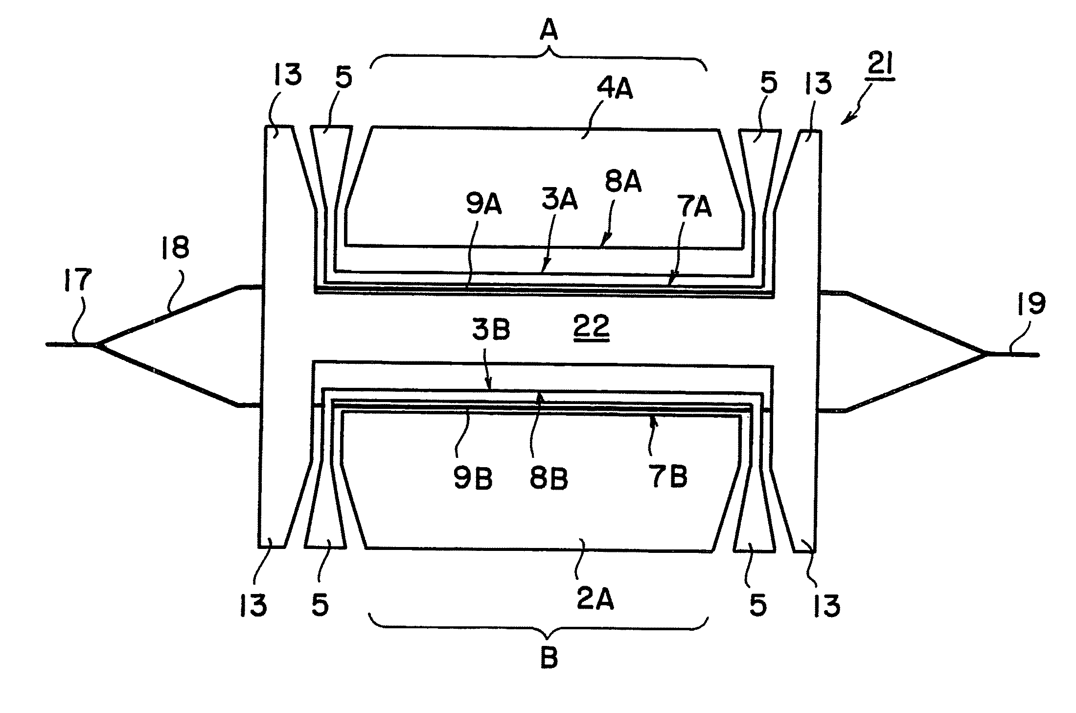
Figure 1 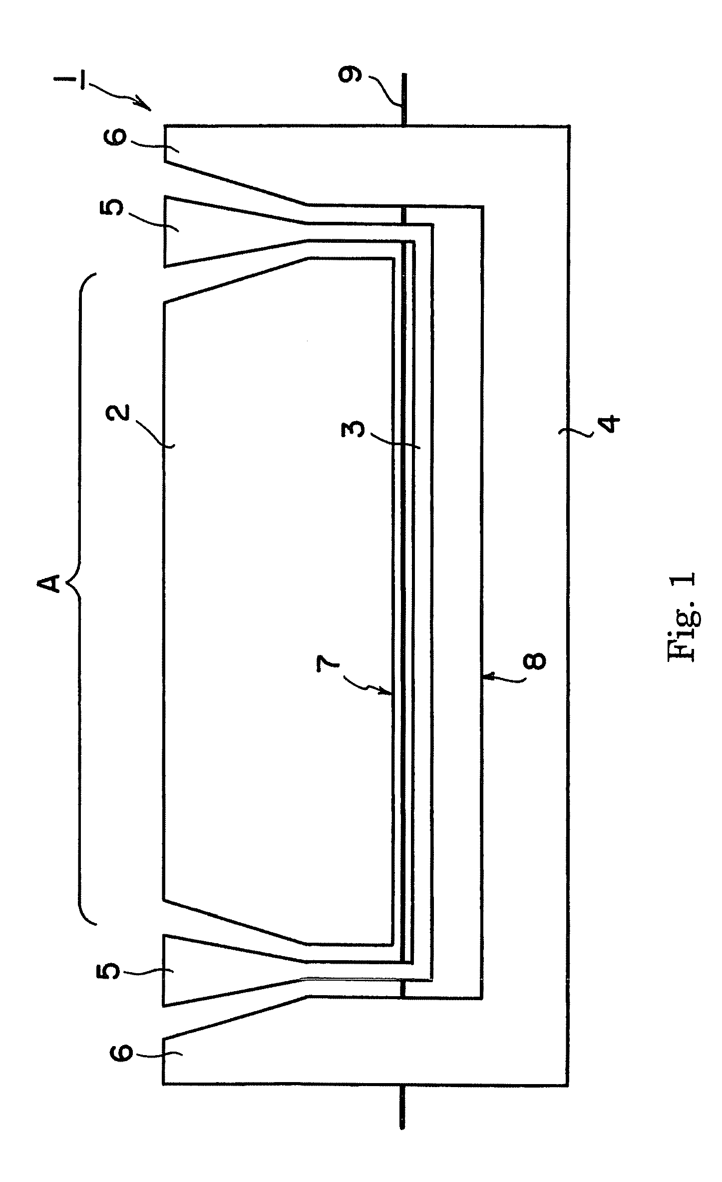
Figure 2 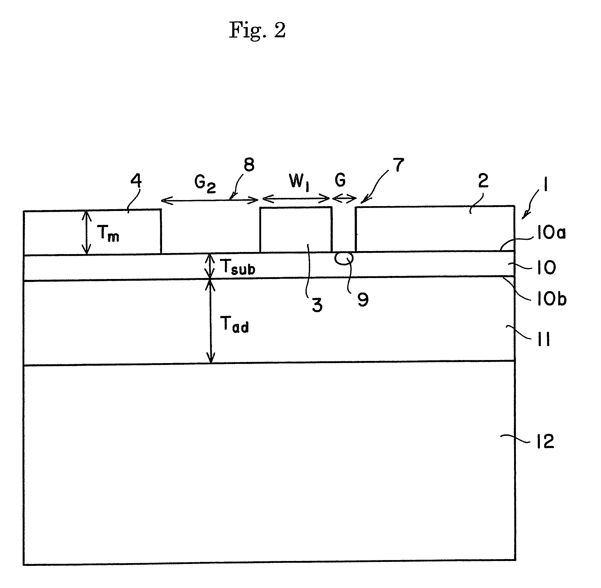
Figure 3
Abstract
Description
TECHNICAL FIELD
[0001] The present invention relates to an optical phase modulator.BACKGROUND ART
[0002] “Band Operation of Guided-Wave Light Modulators with Filter-Type Coplanar Electrodes”, IEICE TRANS. ELECTRON., VOL. E78-C, No. 1, January 1995 discloses a optical phase modulator using so-called ACPS electrodes. In this modulator, a channel optical waveguide is formed between a ground electrode and a signal electrode of the ACPS electrodes, and a voltage is impressed on the optical waveguide, thereby modulating the phase of propagating light.
[0003] On the other hand, Japanese Patent Publication No. H2-269309A describes, in FIG. 9, that, in an amplitude modulator modulating the amplitude of incident light, a modulation voltage is impressed from asymmetric coplanar electrodes on a pair of branched waveguides of a Mach-Zehnder optical waveguide. In this type of electrodes, the respective widths of pair of gaps are different from each other.
[0004] Japanese Patent Publication No. 2005-91698...
Examples
first example
[0069]The optical phase modulator 1 as shown in FIGS. 1 and 2 was produced, and a phase modulation experiment was carried out. Sizes are set as follows (refer to FIG. 2).
[0070]G1=16 μm, G2=92 μm, W=38 μm, Tm=20 μm,
[0071]Tsub=7.0 μm, Tad=50 μm, and relative permittivity of the low dielectric constant layer 11: 4.0.
[0072]As the electric-optical substrate 10, an X-cut lithium niobate substrate was used. With this structure, the effective refractive index of microwave was 2.2, and the microwave and light are velocity-matched. The characteristic impedance was 43Ω. Moreover, the half-wave voltage Vπ decreased down to 3.3V when the interaction-length of the electrodes was 32 mm.
second example
[0073]The optical phase modulator 21 as shown in FIGS. 3 and 4 was produced, and a phase modulation experiment was carried out. It should be noted that the following dimensions were set.
W=40 μm, G1=16.5 μm, G2=90 μm,
WGND=WGND2=WGND3=100 μm, Tsub=7 μm,
electrode thickness Tm=17 μm, and electrode interaction length L=3.2 cm.
[0074]As the electric-optical substrate 1, an X-cut lithium niobate substrate was used. With this structure, the effective refractive index of microwave was 2.2, and the microwave and light are velocity-matched. The following data were obtained under these conditions.
[0075]Electrode conductor loss α=0.33 dB·cm−1·GHz−1 / 2
[0076]Characteristic impedance Z=41 Ω
[0077]Half wave voltage Vπ=3.4 V
[0078]Product of half wave voltage and interaction length VπL=10.8 V·cm
[0079]3 dB band width ΔF3 dB=25 GHz
third example
[0080]Dependency on the ground electrode width WGND was investigated in the second example. In other words, in FIG. 4, only WGND was variously changed. As a result, when the ground electrode widths WGND were 50, 150, 200 and 500 μm, the electrode propagation loss α were respectively 0.34, 0.32 and 0.31 dB·cm−1·GHz−1 / 2. Even when WGND is decreased down to approximately 50 μm, it is appreciated that the electrode propagation loss does not change so much.