
Packaged power semiconductor device
a semiconductor device and power semiconductor technology, applied in semiconductor devices, semiconductor/solid-state device details, electrical equipment, etc., can solve problems such as the risk of damaging other circuit components
Patent Information
- Authority / Receiving Office
- US · United States
- Patent Type
- Applications(United States)
- Current Assignee / Owner
- Publication Date
- 2022-08-11
Smart Images
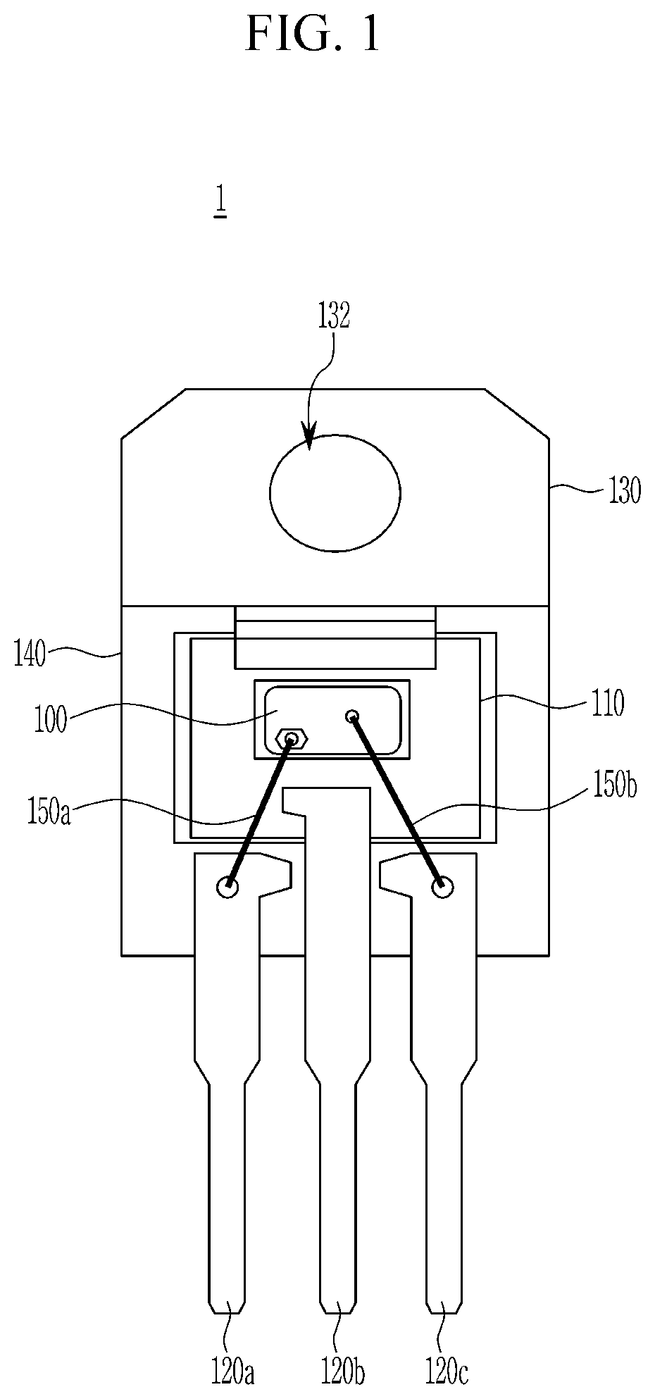
Figure 1 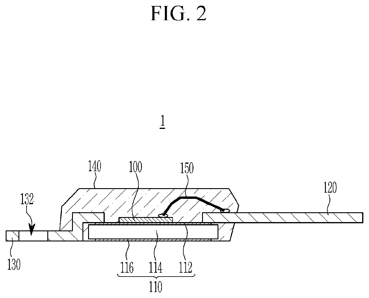
Figure 2 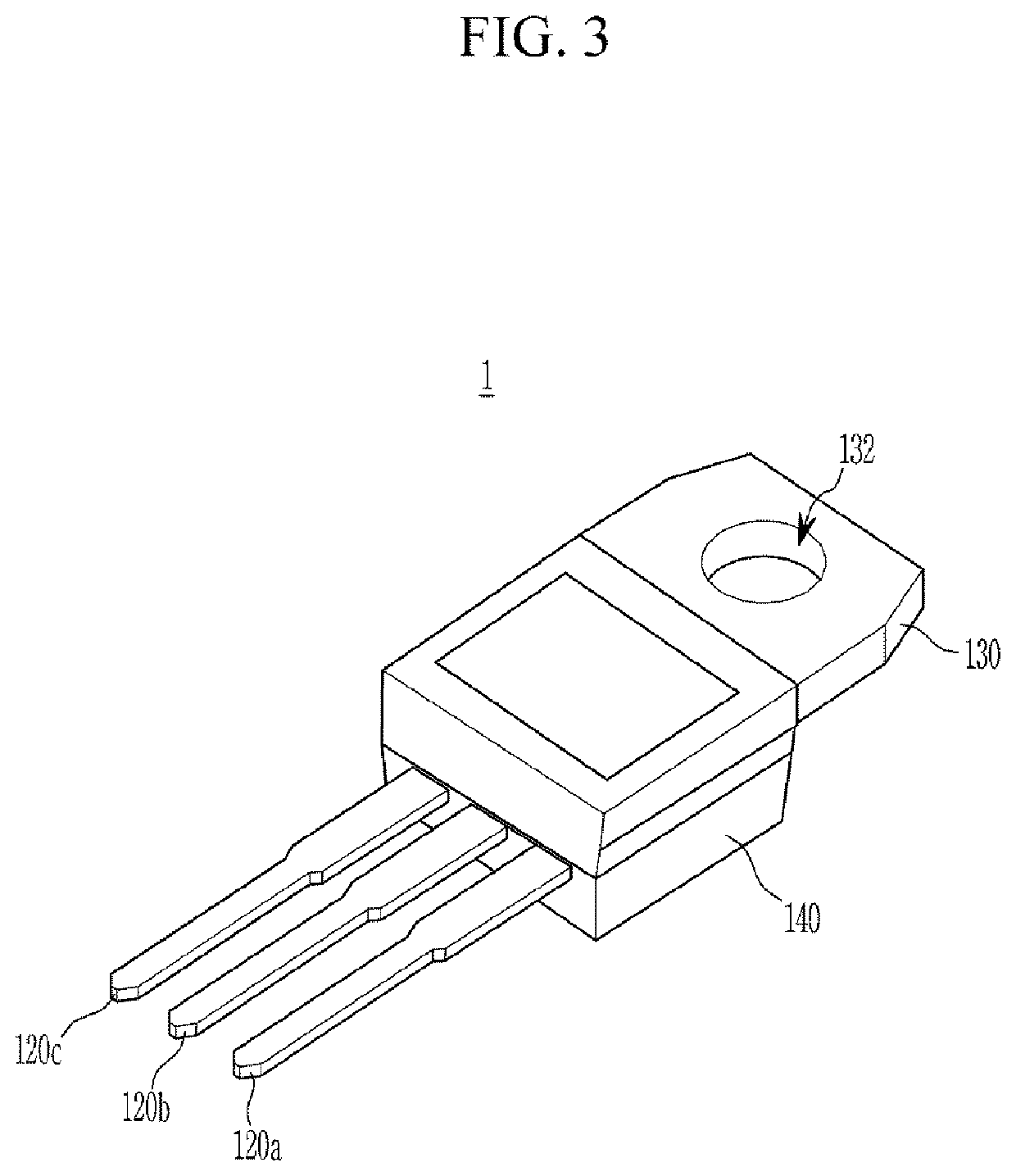
Figure 3
Abstract
Description
CROSS-REFERENCE TO RELATED APPLICATION
[0001] This application claims priority to and benefits of Korean Patent Application No. 10-2021-0016966, filed in the Korean Intellectual Property Office on Feb. 5, 2021, the entire contents of which are incorporated herein by reference.BACKGROUND OF THE DISCLOSURE(a) Field of the Disclosure
[0002] The present disclosure relates to a packaged power semiconductor device.(b) Description of the Related Art
[0003] A power semiconductor device such as a silicon controlled rectifier (SCR), an insulated gate bipolar transistor (IGBT), a silicon carbide (SiC), a field effect transistor (FET), a metal oxide semiconductor field effect transistor (MOSET), a power rectifier, and a power regulator operate at a relatively high voltage, but is assembled in a package that is not electrically isolated. In general, metal tabs forming a rear surface of the package are electrically connected to a semiconductor chip (or semiconductor die), and thus a potential of the re...
Examples
Embodiment Construction
[0024]Hereinafter, the present disclosure will be described more fully with reference to the accompanying drawings, in which embodiments of the disclosure are shown. As those skilled in the art would realize, the described embodiments may be modified in various different ways, all without departing from the spirit or scope of the present disclosure. Accordingly, the drawings and description are to be regarded as illustrative in nature and not restrictive. Like reference numerals designate like elements throughout the specification. In addition, throughout the specification and claims, unless explicitly described to the contrary, the word “comprise” and variations such as “comprises” or “comprising” will be understood to imply the inclusion of stated elements but not the exclusion of any other elements.
[0025]FIG. 1 to FIG. 3 illustrate views for describing a packaged power semiconductor device according to an embodiment of the present disclosure.
[0026]Referring to FIG. 1 to FIG. 3, t...