

Cleaning equipment of semiconductor silicon chip and cleaning method thereof
A technology for cleaning equipment and semiconductors, which is applied in the directions of cleaning methods using liquids, cleaning methods using gas flow, cleaning methods and utensils, etc., which can solve the problem of high cost of cleaning equipment, reduce equipment costs, ensure production capacity, and improve production efficiency. Effect
- Summary
- Abstract
- Description
- Claims
- Application Information
AI Technical Summary
Problems solved by technology
Method used
Image

Examples
Embodiment Construction
[0026] The semiconductor silicon wafer cleaning equipment and cleaning method proposed by the present invention will be further described in detail below in conjunction with the accompanying drawings and specific embodiments. Advantages and features of the present invention will be apparent from the following description and claims. It should be noted that the drawings are all in a very simplified form and use imprecise ratios, which are only used to facilitate and clearly assist the purpose of illustrating the embodiments of the present invention.
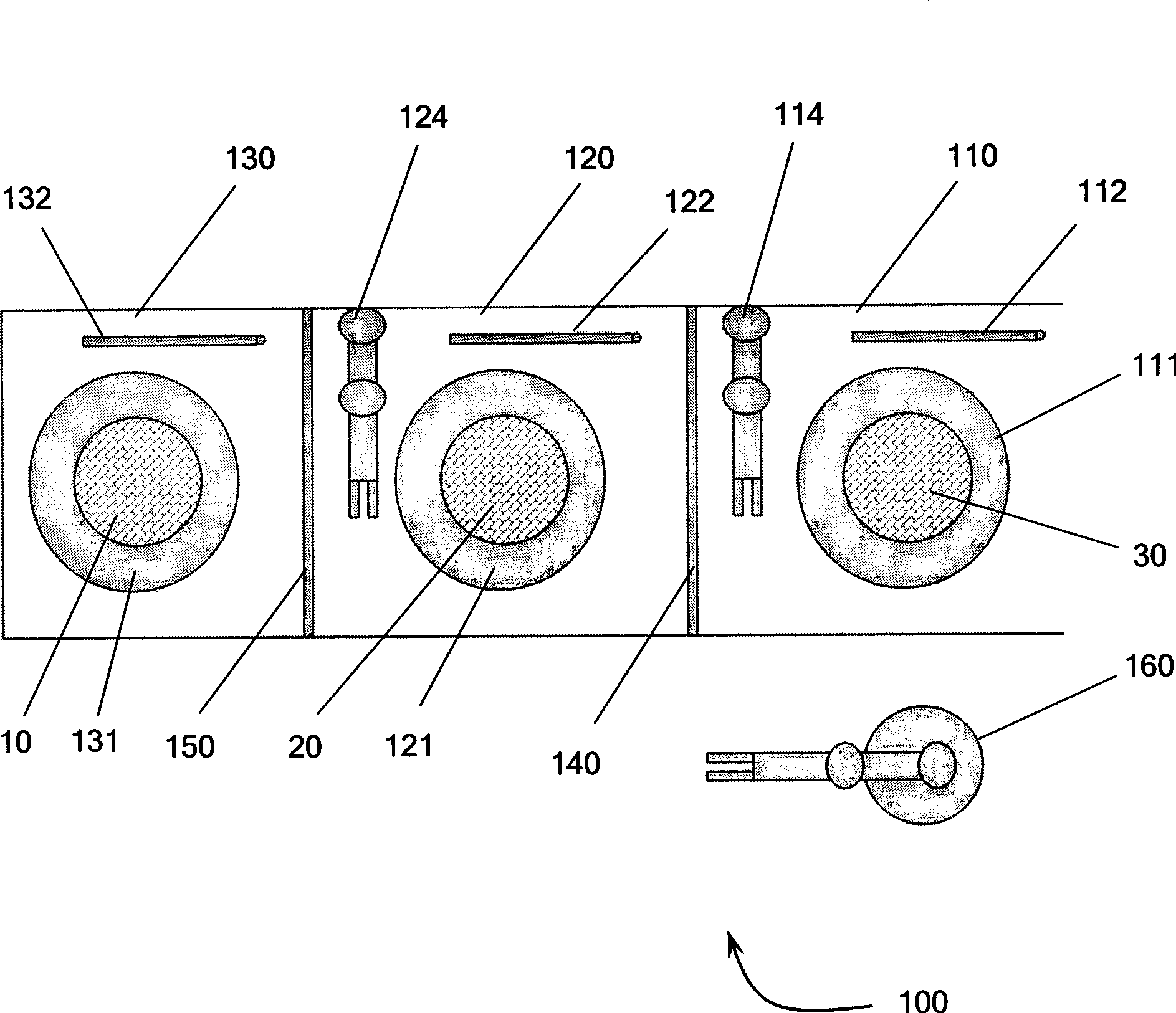
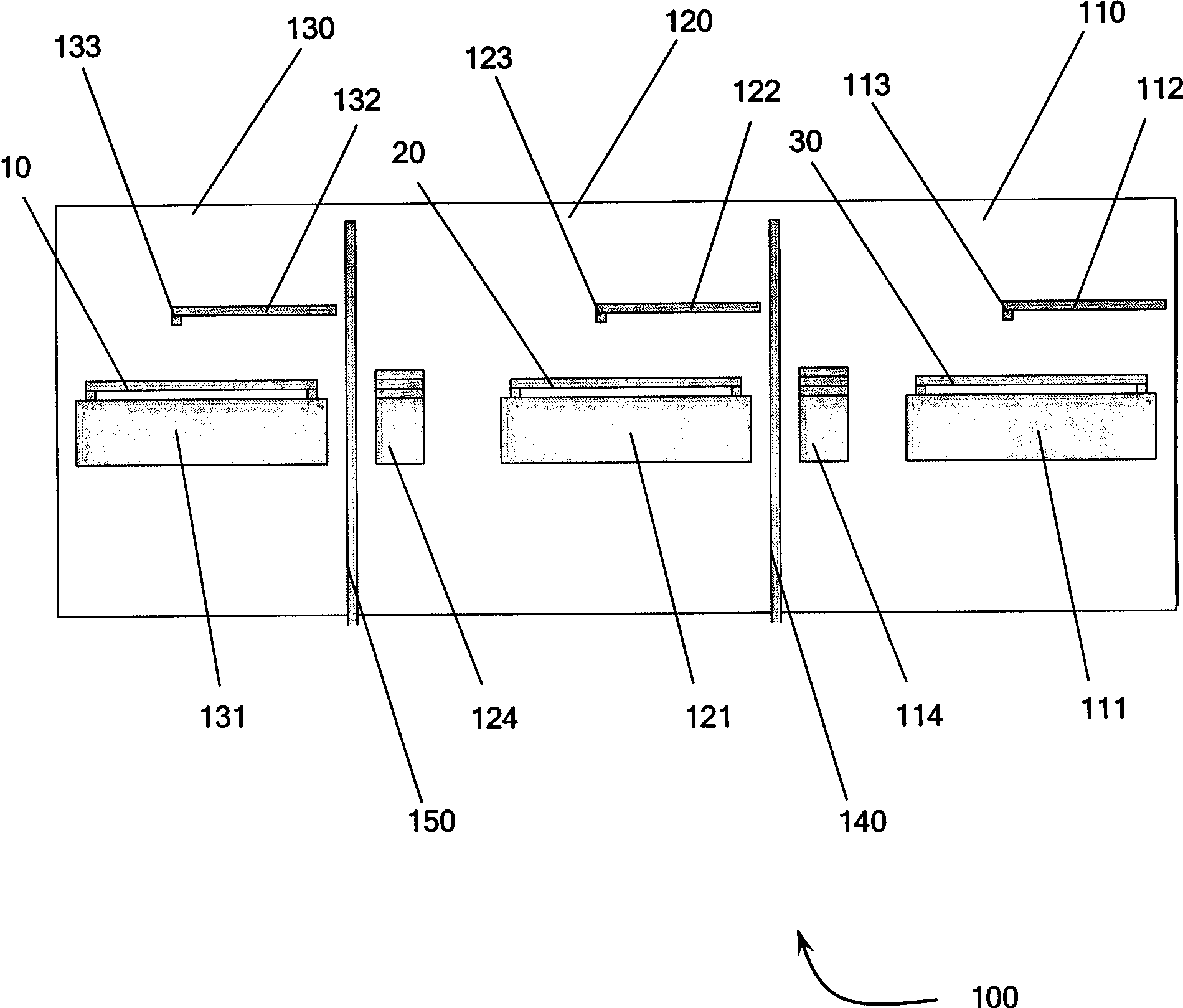
[0027] Please refer to Figure 1A to Figure 1B , which is a schematic diagram of semiconductor silicon wafer cleaning equipment provided by an embodiment of the present invention, wherein Figure 1A For a top view diagram, Figure 1B It is a schematic side view, the semiconductor silicon wafer cleaning equipment 100 includes a plurality of process chambers connected in series to perform a cleaning process, and the cleaning proces...
PUM
| Property | Measurement | Unit |
|---|---|---|
| Rotation angle | aaaaa | aaaaa |
Abstract
Description
Claims
Application Information