Liquid crystal display panel and manufacturing method thereof
A technology of liquid crystal display panel and manufacturing method, which is applied in semiconductor/solid-state device manufacturing, optics, instruments, etc., can solve the problems of large non-display area, small signal attenuation, small non-display area, etc., to achieve small area and attenuation small effect
- Summary
- Abstract
- Description
- Claims
- Application Information
AI Technical Summary
Problems solved by technology
Method used
Image

Examples
Embodiment Construction
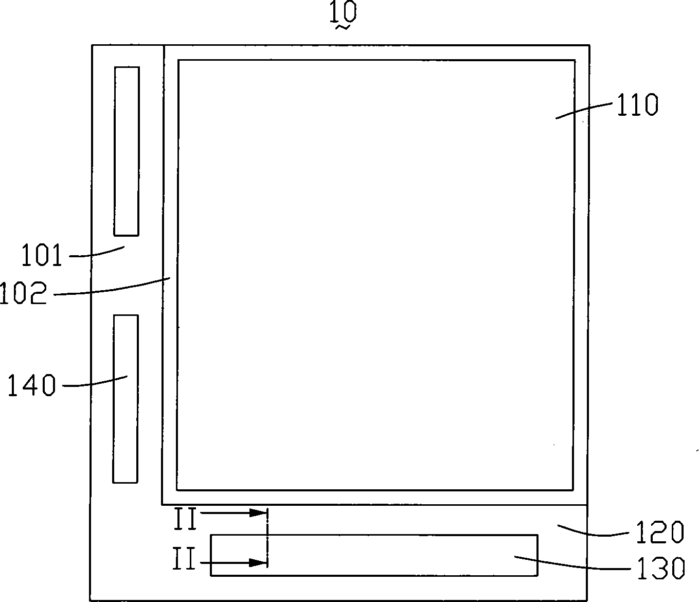
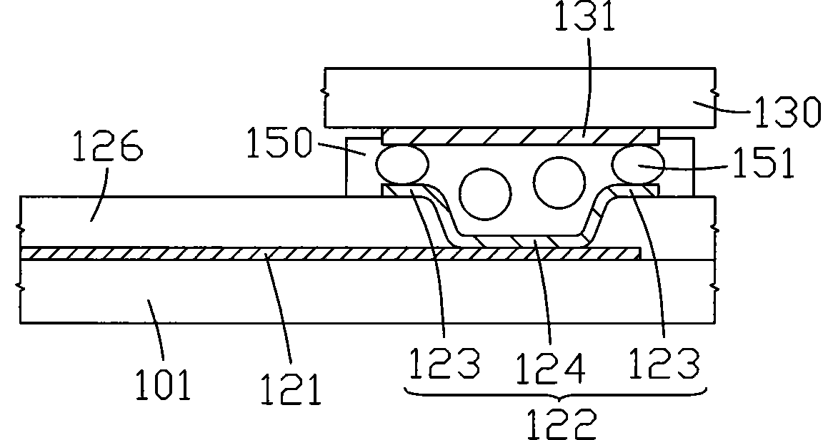
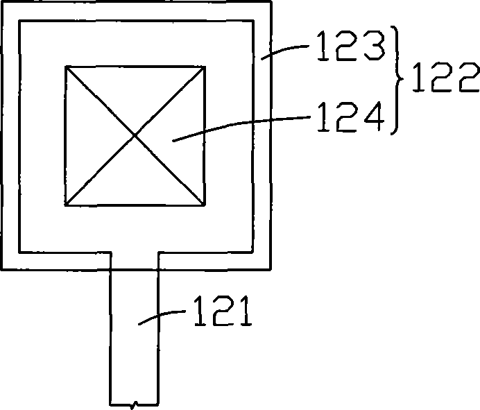
[0031] see Figure 6 and Figure 7 , Figure 6 is a schematic plan view of the first embodiment of the liquid crystal display panel of the present invention, Figure 7 yes Figure 6 The schematic cross-sectional view of the liquid crystal display panel along the VII-VII direction is shown. The liquid crystal display panel 30 includes a TFT substrate 301 and a color filter substrate 302 . The color filter substrate 302 is disposed opposite to the TFT substrate 301 and has an area smaller than that of the TFT substrate 301 . A portion of the TFT substrate 301 overlapping the color filter substrate 302 defines a display area 310 , and a portion of the TFT substrate 301 not overlapping the color filter substrate 320 defines a non-display area 320 . A liquid crystal layer 303 is disposed between the TFT substrate 301 and the color filter substrate 302 corresponding to the display area 310 .
[0032] The non-display area 320 includes a scan driver 330, two data drivers 340, a ...
PUM
| Property | Measurement | Unit |
|---|---|---|
| size | aaaaa | aaaaa |
Abstract
Description
Claims
Application Information