Check patentability & draft patents in minutes with Patsnap Eureka AI!

Semiconductor layer, method of manufacturing the same, laser diode, and method of manufacturing the same

一种制造方法、半导体的技术,应用在半导体激光器、半导体/固态器件制造、激光器等方向,能够解决激光器可靠性受损、晶体缺陷增加等问题,达到抑制杂质失去活性的效果

Active Publication Date: 2010-10-20
SONY CORP
View PDF9 Cites 1 Cited by
  • Summary
  • Abstract
  • Description
  • Claims
  • Application Information

AI Technical Summary

Problems solved by technology

However, if the semiconductor is doped with more impurities than necessary, the impurities will diffuse into the active layer, or crystal defects in the p-type semiconductor will increase
As a result, there is a problem of impaired reliability of the laser

Method used


Image

  • Semiconductor layer, method of manufacturing the same, laser diode, and method of manufacturing the same
  • Semiconductor layer, method of manufacturing the same, laser diode, and method of manufacturing the same
  • Semiconductor layer, method of manufacturing the same, laser diode, and method of manufacturing the same

Examples


Embodiment Construction

[0025] Hereinafter, embodiments of the present invention will be described in detail with reference to the accompanying drawings. Descriptions are given in the following order:

[0026] 1. Structure

[0027] 2. Manufacturing method

[0028] 3. Function and effect

[0029] 1. Structure

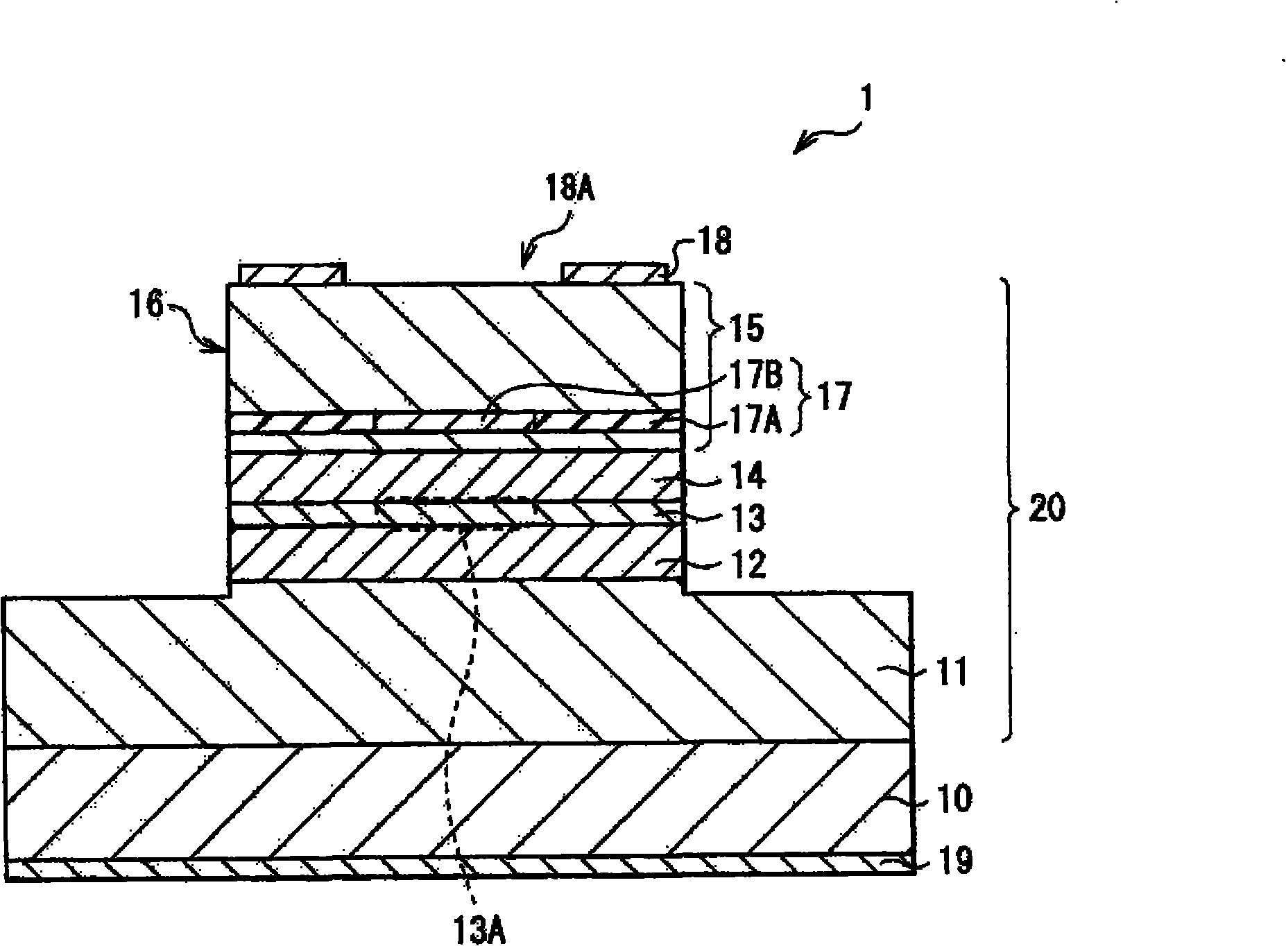
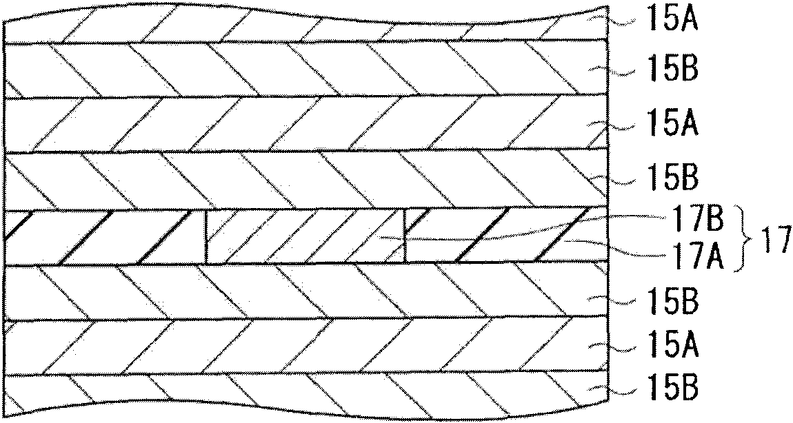
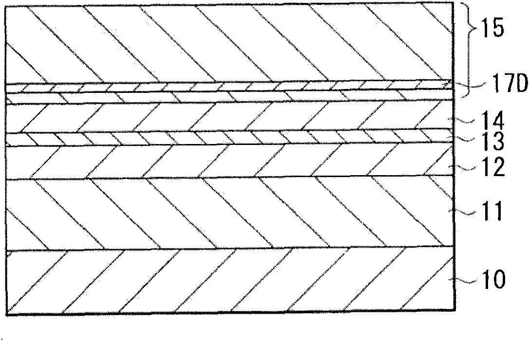
[0030] figure 1 A cross-sectional configuration of a VCSEL according to an embodiment of the present invention is illustrated. figure 1 is a schematic diagram, so the size and shape of the laser 1 are different from the actual size and shape. Laser diode 1 includes stacked structure 20 in which lower DBR layer 11 , lower spacer layer 12 , active layer 13 , upper spacer layer 14 , and upper DBR layer 15 are sequentially stacked on one surface side of substrate 10 . The laminated structure 20 corresponds to a specific example of the "laminated structure" of the present invention. The upper part of the stacked structure 20 , specifically, part of the lower DBR layer 11 , lower spacer layer ...


PUM


Abstract

The invention provides a semiconductor layer, a method of manufacturing the same, a laser diode, and a method of manufacturing the same. The method of manufacturing a semiconductor layer with which inactivation of impurity is able to be inhibited by a simple method, a semiconductor layer in which inactivation of impurity is inhibited, a method of manufacturing a laser diode with which inactivation of impurity is able to be inhibited by a simple method, and a laser diode including a semiconductor layer in which inactivation of impurity is inhibited are provided. In the method of manufacturing a semiconductor layer, after a semiconductor layer is formed by epitaxial growth with the use of AsH3, supply of AsH3 is stopped without separately supplying new gas when process temperature is 500 deg C. or more.

Description

technical field [0001] The present invention relates to a low-resistance semiconductor layer and a manufacturing method thereof, and a laser diode including the low-resistance semiconductor layer and a manufacturing method thereof. Background technique [0002] In the past, it has been known that in p-type semiconductor crystal materials, p-type impurities are deactivated and the carrier concentration is lowered by bonding hydrogen atoms to p-type impurities. A decrease in carrier concentration results in high resistance and a decrease in lifetime due to heat generated at the time of operation, that is, a decrease in reliability. Incorporation of hydrogen at lower temperatures after growth makes long-term stable laser operation difficult. [0003] The deactivation of the p-type impurity is caused by the fact that arsine (AsH 3 ) generated hydrogen radical (hydrogen radical) was introduced into the crystal (see Japanese Patent No. 3553147). Therefore, in order to obtain th...

Claims


Application Information

Patent Timeline
Patent Type & Authority Applications(China)
IPC IPC(8): H01S5/323
CPCH01S2304/04H01S5/32316H01L21/0262H01S2304/00H01S5/3054H01L21/02579H01L21/02546H01S5/18347H01S5/18311H01L21/02395
Inventor 城岸直辉荒木田孝博
Owner SONY CORP
Features
  • R&D
  • Intellectual Property
  • Life Sciences
  • Materials
  • Tech Scout
  • Unparalleled Data Quality
  • Higher Quality Content
  • 60% Fewer Hallucinations
Learn More