

Array substrate and preparation method of array substrate and display device
An array substrate and substrate technology, applied in the field of liquid crystal display, can solve the problems of reduced aperture ratio, increased structural complexity of the backlight module, display device cost, reduced light transmittance, etc., achieving low cost, increased design difficulty, and increased complexity Effect
- Summary
- Abstract
- Description
- Claims
- Application Information
AI Technical Summary
Problems solved by technology
Method used
Image



Examples
Embodiment 1
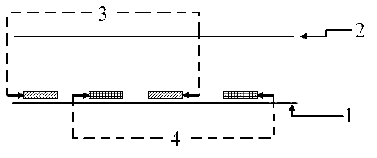
[0026] This embodiment provides an array substrate. The array substrate includes TFTs formed on the substrate and pixel regions arranged on the substrate. The pixel regions are correspondingly provided with a gate insulating layer. The electrode structure adopted by the array substrate is as follows: figure 2 and image 3 As shown, specifically, the first pixel electrodes 3-1 and the first common electrodes 4-1 are alternately arranged on one side surface of the gate insulating layer, and the second pixel electrodes 3-1 are alternately arranged on the other side surface of the gate insulating layer. Two common electrodes 4-2 and the second pixel electrode 3-2, the first pixel electrode 3-1 and the second common electrode 4-2 located on different surfaces are correspondingly arranged up and down, and the first pixel electrodes located on different surfaces The common electrode 4-1 and the second pixel electrode 3-2 are disposed correspondingly up and down; wherein, the polarit...
Embodiment 2
[0032] This embodiment provides a method for preparing an array substrate, which is implemented for the array substrate in Embodiment 2. Specifically, the preparation method includes the following processes:
[0033] TFTs and pixel regions are formed on the substrate, and gate insulating layers are correspondingly formed in the pixel regions, wherein first pixel electrodes and first common electrodes are alternately arranged on one side surface of the gate insulating layers, and the gate insulating layers The second common electrode and the second pixel electrode are alternately arranged on the other side of the surface, the first pixel electrode and the second common electrode on different surfaces are arranged correspondingly up and down, and the first common electrode on different surfaces It is set up and down corresponding to the second pixel electrode; wherein, the polarity of the pixel electrode is opposite to that of the common electrode.
[0034] According to the sett...
Embodiment 3
[0036] This embodiment provides a display device, which includes the array substrate described in Embodiment 1 or the array substrate prepared in Embodiment 2. The display device can be: a liquid crystal panel, an electronic paper, an OLED panel, a liquid crystal TV , liquid crystal display, digital photo frame, mobile phone, tablet computer and other products or components with any display function.
[0037] It can be known from the above embodiments that the present invention arranges alternately arranged pixel electrodes and common electrodes on both sides of the gate insulating layer of the array substrate, and makes the polarities of the pixel electrodes and the common electrodes opposite, and the pixel electrodes and the common electrodes on both sides are up and down. Correspondingly, the electrode structure has both a fringe field and a planar electric field when a voltage is applied, and can be directly driven by the existing driving method in the IPS mode without incr...
PUM
 Abstract
Description
Claims
Application Information