Method for monitoring height of step formed by photosensitive mask etched silicon carbide material in real time

A step height, real-time monitoring technology, applied in semiconductor/solid-state device testing/measurement, etc., to ensure device performance and improve process flow

CN103247549AActive Publication Date: 2013-08-14NO 55 INST CHINA ELECTRONIC SCI & TECHNOLOGYGROUP CO LTD
3 Cites 2 Cited by

Patent Information

Authority / Receiving Office
CN · China
Current Assignee / Owner
Publication Date
2013-08-14

Smart Images

  • Figure 1
    Figure 1
  • Figure 2
    Figure 2
  • Figure 3
    Figure 3
Patent Text Reader

Abstract

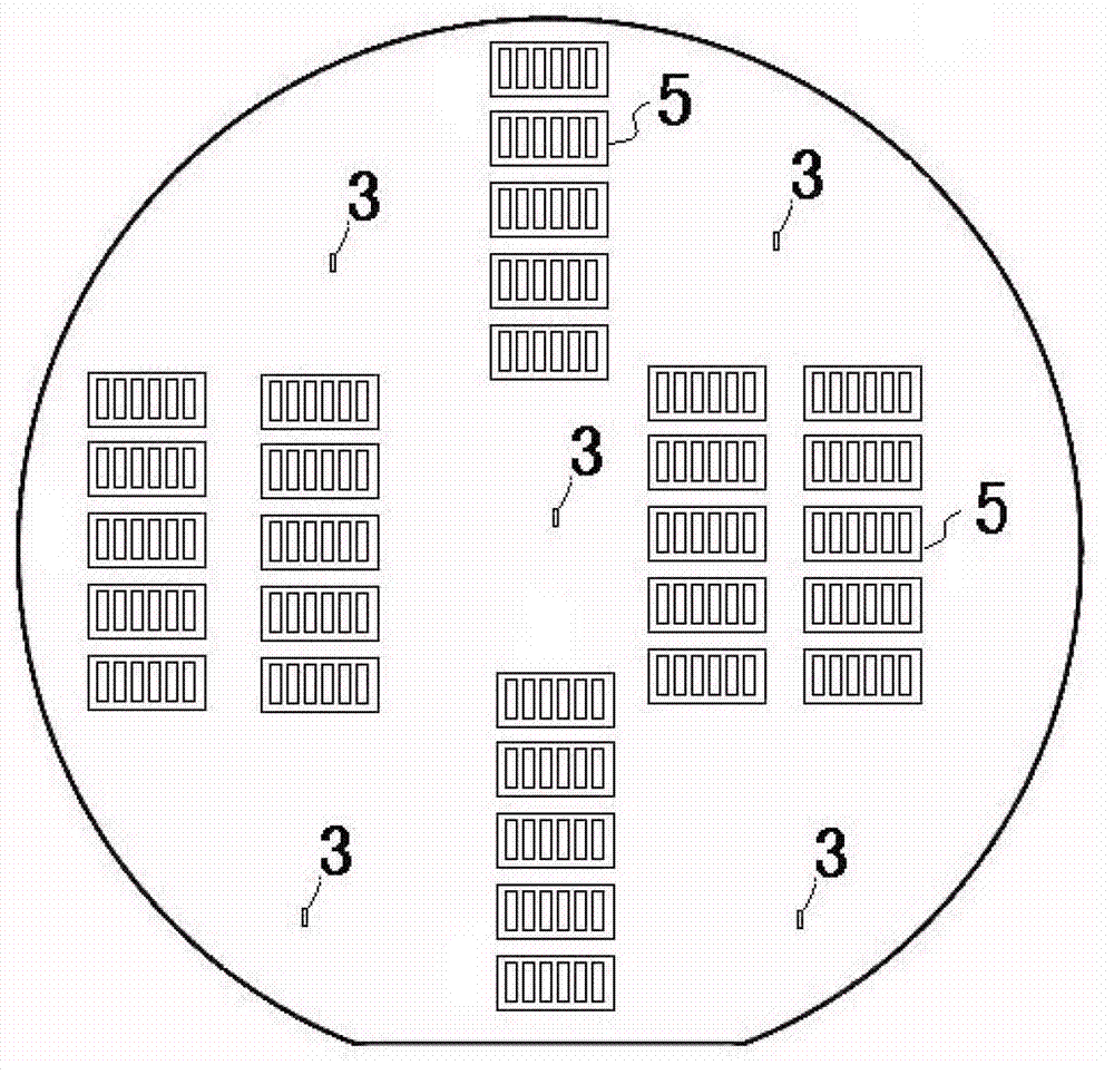
The invention discloses a method for monitoring the height of a step formed by photosensitive mask etched silicon carbide material in real time, the method comprises the following steps: a plurality of step height monitoring patterns are arranged on a silicon carbide material and are etched together with to-be-etched patterns, when the etching height is required to be detected, the photosensitive mask layer on the periphery of one of step height monitoring patterns is removed, so that monitoring of step height is performed. The method ensures real time monitoring and precision control of step height when the silicon carbide is etched through a drying method by utilizing a manner that the step height monitoring pattern areas are not developed after being exposed for many times, thereby effectively ensuring improvement of the performance of devices and operation of process flow.
Need to check novelty before this filing date? Find Prior Art

Description

technical field

[0001] The invention relates to the technical field of metal silicon carbide etching, in particular to a method for real-time height monitoring of steps formed by etching silicon carbide materials using a photosensitive mask. Background technique

[0002] Silicon carbide (SiC), a wide bandgap semiconductor material, has the characteristics of wide bandgap width, high critical field strength, high thermal conductivity, and high carrier saturation rate. SiC epitaxy on SiC substrate is the most important semiconductor material for manufacturing high temperature, high frequency, high power devices, etc. It has super performance and broad application prospects. In SiC devices, various steps of different heights that need to be precisely controlled are commonly used structures in the manufacture of various transistor processes, so how to monitor the step height in real time in the manufacture of steps with micron-scale line widths is one of the key processes to ach...

Examples

Embodiment Construction

[0028] Below in conjunction with specific embodiment, further illustrate the present invention, should be understood that these embodiments are only used to illustrate the present invention and are not intended to limit the scope of the present invention, after having read the present invention, those skilled in the art will understand various equivalent forms of the present invention All modifications fall within the scope defined by the appended claims of the present application.

[0029] A silicon carbide photosensitive mask etching method for real-time monitoring of step height, the specific steps are as follows:

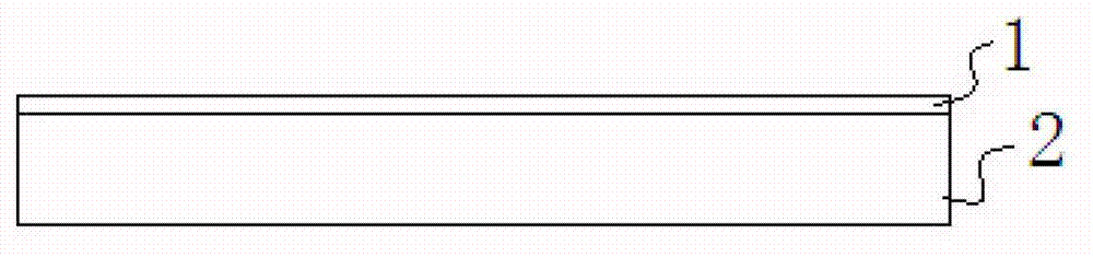
[0030] 1. Use an acid solution to clean the silicon carbide material 1; the acid solution uses hydrochloric acid and pure water, and the weight ratio of hydrochloric acid and pure water is 1:5; the silicon carbide material 1 is a silicon carbide epitaxial wafer; figure 1 shown

[0031] 2. Coating the adhesive and photosensitive mask layer 2 on the silicon carbi...